Downloads #
Introduction #
Microcontroller Display Module for Electronics Education is a key nowadays. The purpose of the PRESSON Microcontroller Display Module is to is to provide a convenient platform for indicating output data produced by the PRESSON C51 Microcontroller Project Launcher. The display module performs two basic functions:
• Eight red LEDs and their associated transistor driver circuitry provide a quick and easy means of displaying the status of up to eight bits of data, such as a byte of output data from either Port 0 or Port 1 of the C8051F330-GM MCU contained on the C51 Microcontroller Project Launcher.
• Three seven-segment displays, located on the ground plane side of the circuit module, allow the display of three BCD numerals in a decimal format. Decoder/driver and demultiplexing circuitry on the silkscreen side of the Microcontroller Display Module allow the three-digit display and demultiplexer to be controlled via just seven pins (bits 0 through 6) of Port 1 of the C8051F330GM MCU.
The PRESSON Microcontroller Display Module is designed for use by the student who has completed Unit 1 of Course PCMT2C1 (Introduction to Eight-Bit Microcontrollers) and is ready to delve into microcontroller interfacing. Unit 2 of that course contains experimental procedures demonstrating methods of interfacing the C51 Microcontroller Project Launcher with the Microcontroller Display Module. Assembly language code examples are introduced that demonstre the enabling of individual bit positions of Ports 0 and 1 to become inputs to the eight LED drivers of the display module. Next, more advanced coding examples are introduced, demonstrating the ability of the project launcher to multiplex four bits of data and send them to display demultiplexer and encoder/decoder circuitry contained on the display board.
Printed Circuit Board Specifications: #
Microcontroller Display Module for Electronics Education represents The Microcontroller Display Module and its contained on a 4.5″ x 2.3″ two-layer FR-4 epoxy glass PCB (printed circuit board) with 1/2 oz copper laminate. Both sides of the PCB are coated with solder mask to prevent damage by oxidation and limit the occurrence of solder bridges during assembly. The lower layer of the PCB contains a ground plane, with thermal pads for connection of components to the common 0.0VDC reference. Four pads with a 0.125″ inner diameter, located at the four corners of the PCB, serve as mounting holes. These pads connect directly to the PCB ground plane, allowing the board to be mounted on a metal panel and provide a common connection to a chassis ground point. (Aluminum standoffs and mounting hardware are included with the Microcontroller Display Module Ancillary Kit.) Figure 1 contains a silk screen view of the upper layer of the PCB, clearly indicating the location of each component. The locations of Display1 and Display2 are shown on the silk screen side of the board. However, these components are mounted on the opposite, ground plane side of the PCB.
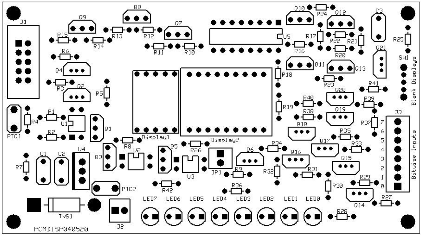
Figure 2 uses colors to represent the two layers of the Microcontroller Display Module. Here, the ground plane and traces on the lower layer of the circuit board are represented in green, while traces, pads, and vias on the upper layer of the board are shown in red. The locations of components on the upper, silk screen layer of the PCB are shown in yellow.
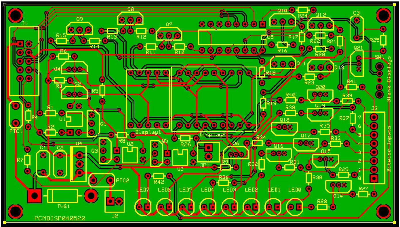
Table 1 identifies and defines several of the reference designators used for components contained on PRESSON Circuit Modules products.
| Table 1 – Common Component Designators | |
|---|---|
| Designation | Description |
| J (J1, J2, J3…) | Input/Output Connector |
| TP (Tp1, TP2, TP3…) | Test Point |
| JP (JP1, JP2, JP3…) | Jumper Position |
| R (R1, R2, R3…) | Resistor |
| C (C1, C2, C3…) | Capacitor |
| L (L1, L2, L3…) | Inductor |
| U (U1, U2, U3…) | Integrated Circuit (IC) |
| Q (Q1, Q2, Q3…) | Transistor |
| LED (LED1, LED2…) | Light Emitting Diode |
| PTC (PTC1, PTC2…) | Resettable Fuse |
| RT (RT1, RT2, RT3) | Thermistor |
| K (K1, K2, K3…) | PCB Relay |
| SW (SW1, SW2…) | Switch |
Microcontroller Display Module Interconnect: #
The Microcontroller Display Module, designed to work in conjunction with the C51 Microcontroller Project Launcher, receives DC voltage from that module via either a ten-position ribbon cable or through a two-wire daisy chain +12.0VDC connection. These options for connecting power to the Microcontroller Display Module are illustrated in Figure 3.


The most convenient method of connecting DC voltage from the project launcher and display module is via the ten-position ribbon cable. Figures 3-a and 3-c, as well as the photographs in Figures 3-d and 3-e, illustrate this interconnect option. Connector J5, located in the lower RH corner of the project launcher is a dual row, ten-position JTAG header that provides Power_In (typically +12.0VDC), +3.0VDC, and a common ground connection to a right-angled JTAG connector located at the upper LH side of the display module. Header J5 on the project launcher also provides access to bit 0 through bit 6 of port 1 of the C8051F330-GM MCU. These seven bit positions are used in controlling the demultiplexer circuitry for the three seven-segment displays on the ground plane side of the display module.
NOTE: JTAG is an acronym for the Joint Test Action Group, which codified a standard method of verifying proper operation of printed circuit boards. The JTAG pin-strip header has become a standard form of connector for debugging and in-system programming (ISP) of microcontrollers.
If the user application is limited to operation of only the eight LED drivers of the display module, Power_In and ground can be easily daisy chained from the project launcher. As shown in Figure 3-b, three-position header J10 of the project launcher connects easily to the two-position header J2 on the display module, using two female-to female jumpers. Connecting a jumper from pin 1 of J10 of the project launcher to pin 1 of J2 of the display module completes the Power_In link. Connecting a jumper from pin 2 or 3 of J10 project launcher to pin 2 of J2 of the display module provides ground continuity. (The display module does not require a +3.3V connection for operation of the LED drivers.)
Microcontroller Display Module DC Voltage Distribution: #
Figure 4 shows the DC voltage distribution for the Microcontroller Display Module. The source voltage at the board Power_In pins could range from +9.0VDC to +18.0VDC but is assumed to be +12.0VDC if derived from the C51 Microcontroller Project Launcher Module. In Figure 4, pads connecting components to the +12.0VDC bus are highlighted in pale blue. PTC1 and PTC2 are resettable fuses (or polyswitches) that protect the +12.0VDC (Power_In) bus from an over-current condition. Assuming input current at pin 1 of J1 remains below a holding level of 500mA, PTC1 behaves as a closed switch, offering virtually zero ohms of resistance. Once current exceeds the 500mA limit, PTC1 trips into a high impedance state, inhibiting further flow of input current. PTC2 performs the same current limiting action for a daisy chained power input taken at header J2. Once either resettable switch is tripped, power must be removed from the module and the over-current condition must be remedied before normal operation can resume. Note, as indicated in Figure 4, if the +12.0VDC input is taken at pin 1 of J1, J2 can provide a +12.0VDC daisy-chained output.
The Microcontroller Display Module receives +3.3VDC at pin 4 of JTAG header J1. In Figure 4, pads connecting components to the +3.3VDC bus are highlighted in white. The +3.3VDC input is required for operation of the optocouplers (U1, U2, and U3) and transistor switches contained in display demultiplexer circuitry. Also, +3.3VDC becomes VDD for the CMOS BCD to 7-segment decoder/driver IC (U5).

In Figure 4, pads connecting components to the +5.0VDC bus are highlighted in orange. The +5.0VDC bus functions as VCC for the eight common emitter transistor switches serving as drivers for the eight LED indicators (LED0 through LED7). The optocouplers and transistor switches contained in the display demultiplexer circuitry also require +5.0VDC.

The Microcontroller Display Module does not receive +5.0VDC directly from the C51 Microcontroller Project Launcher. Instead, as shown schematically in Figure 5, 500mA linear voltage regulator U4 reduces the Power_In voltage to a fixed +5.0VDC. As explained earlier, resettable fuse PTC1 limits current flow on the internal +12VDC bus (labelled here as Display_Power_In). C1 is a 0.33μF MLCC (multilayer chip capacitor) which serves as a noise filter, attenuating any high frequency interference that could be present on the +12VDC bus. TVS1 is a transient voltage suppressor, the purpose of which is to clip any high voltage transients that could be present on the +12VDC bus. C2 is a 0.47μF MLCC which serves as a noise filter and stabilizing capacitor for the +5.0VDC bus.
Microcontroller Display Module Indicator LED Driver Circuitry: #
Figure 6 shows the orientation of the eight bitwise LED indicators (LED0 through LED7) on the Microcontroller Display Module. These indicators are low-power, red tinted, 5mm diffused LEDs, rated at only 2.0mA of operating current. They are easily inserted into right-angled LED sockets, allowing observation by the user seated at a workstation. With the component (silk screen) side of the display module facing upward as shown in Figure 6, LED0 holds the least significant bit (LSB), representing 20. LED7 holds the most significant bit (MSB), representing 27.

The drivers for the LED indicators of the Microcontroller Display Module are easily accessed via right-angled eight-position header J3, located in the lower right-hand corner of the display module (viewing the silk screen side). As illustrated in Figure 7, assume the program being executed by the C8051F330-GM microcontroller sends a logic high to its P1.2 output (third bit position of Port 1). This signal is accessible at pin 3 of eight-position header J4 on the C51 Microcontroller Project Launcher. With a female-to female jumper connected between pin pin3 of J4 on the project launcher and pin 3 of J3 on the display module, as indicated in Figure 7, nearly +3.0VDC is present at the base input to switching transistor Q16. (With this example, it is assumed there is already a Power_In and ground connection between the two modules.)
The current flow into the base of Q16 can be estimated assuming VBE to be 0.7V. With R31 equaling 90KΩ, base current is determined as (+3.0V – 0.7V)/ 90KΩ, or approximately 26μA. Per the datasheet for the TLLR5401 LED, its forward voltage drop (VF) is nearly 2.4V at the rated current of 2.0mA. Assuming base current is sufficient to drive Q16 into saturation, its VCE is estimated to be 0.2V. With the collector resistor R32 equaling 1.5KΩ, we can apply Kirchhoff’s and Ohm’s laws to estimate collector current for Q16. VRC = (5.0VDC – 2.4V – 0.2V) = 2.4V. Applying Ohm’s law, IC = 2.4V/1.5KΩ = nearly 1.6mA (slightly less than the rated current for the TLLR5401 LED).

Microcontroller Display Module Seven-Segment Display Demultiplexer: #
In communication electronics, multiplexing is a process in which several signals share a common (single) channel. Control of the three seven segment displays on the Microcontroller Display Module is accomplished through a relatively simple form of time division multiplexing. This process allows illumination of the twenty-one individual LED segments contained in Display1 and Display2 to be controlled by just seven bits of Port 1 of the C8051F330-GM microcontroller. The ten-position ribbon cable connection between the C51 Microcontroller Project Launcher and the Microcontroller Display Module has already been introduced. As shown in Figures 3-d and 3-e, pins 1, 2 and 4 of the ribbon cable are dedicated to routing Power_In (+12.0VDC), ground, and +3.3VDC from the project launcher to the display module. The seven bit positions of Port 1 of the C8051F330-GM microcontroller dedicated to operation of the three displays are routed to the display module via the remaining conductors of the ribbon cable.
As
As shown in Figure 8, bits P1.0, P1.1, P1.2, and P1.3 of Port 1 of the C8051F330-GM microcontroller form a binary coded decimal (BCD) nibble, which can range from 0000 through 1001 (equivalent to decimal 0 through 9). These bits become inputs A, B, C, and D (D0, D1, D2, and D3) to U5, a CD74HC4543 CMOS BCD to 7-segment 12 | P a g e
decoder/driver. The Mouser Electronics part number for this device is 595-CD74HC4543E. Clicking on this part number provides a link to the datasheet for the product.
The CD74HC4543 IC contains complex combinational logic circuitry that reads the BCD input nibble and forms a seven-bit output that corresponds to the seven segments (a through g) within a display. For example, to form the number 3, segments a, b, c, d, and g would illuminate, while segments e and f would be off. For this to occur, outputs a through g of U5 would have formed the number 1111001. (A logic high represents an illuminated segment, while a 0 represents an off condition for the segment.) Page 2 of the CD74HC4543 datasheet contains a Functional Diagram, which serves as a truth table for the CD74HC4543. This table identifies all the possible input combinations to the IC and indicates the resultant output conditions. Note that if the four BCD input bits (A, B, C. and D) exceed 1001 (indicated as HLLH in the table), the seven segment control outputs are held low. This action, of course, blanks the display.

If the CD74HC4543 decoder is being used to control a liquid crystal display (LCD), a square wave is fed to the phase (PH) input at pin 6. This pulsing action is not a requirement when controlling an LED seven segment display so, as shown in Figure 8, the PH input is disabled by connecting it to circuit ground. The LD input at pin 1 is an active-low latching control signal. When pulled to a logic low, the LD signal keeps the seven outputs of the IC at the levels they held prior to a high-to-low transition at pin 1. Because the latching action is not required in the display demultiplexing routine, the LD input is held at nearly +3.3V by pull-up resistor R24.
The Microcontroller Display Module does make use of the blanking input (BI) signal at pin 7 of U5. If the user wants to temporarily disable operation of the seven-segment display circuitry, possibly while working with only the eight LED indicators, he can actuate slide switch SW1 in the direction of J3, which brings pin 7 of U5 to nearly +3.3V. With this condition, all three seven-segment displays are blanked, regardless of activity at inputs P1.0 through P1.6. Actuation of SW1 in the direction of R25 holds pin 7 of U5 at 0 volts, enabling illumination of the displays.
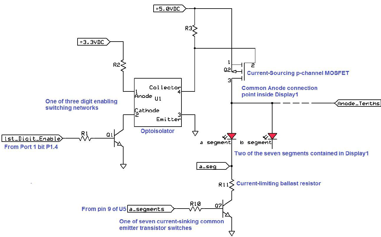
Now that the function of microcontroller port bits P1.0, P1.1, P1.2, and P1.3 has been discussed and the operation of the CD74HC4543 decoder/driver has been explained in detail, the role of transistor switches in controlling the overall operation of the demultiplexer system will be examined. Figure 9 contains a portion of the switching circuitry controlling Display1, the seven-segment display representing the Tenths position. Because the switching circuitry controlling the Ones and Tens displays is identical to that shown here, a detailed analysis of this circuitry is beneficial in understanding the overall timing of the entire multiplexing/demultiplexing system.
While Port 1 bit positions P1.0, P1.1, P1.2, and P1.3 define the value of the BCD nibble being sent to the displays, P1.4, P1.5, and P1.6 determine which of the three seven-segment displays is enabled to operate. The microcontroller program controlling multiplexer operation only allows one of the three enabling bits to be at a logic high at a given instant. Typically, the code utilizes one of the onboard timers of the microcontroller to determine the enabling period of each digit, typically only a few milliseconds. As an example, the repeating commutation cycle for the three port bits (from P1.6 to P1.5, to P1.4) could be: 001, 010, 100, 001, 010, 100, 001, 010, 100…… While the digits are illuminating individually, the action occurs so rapidly that all three displays appear to be illuminated at the same time.
The user has the option of enabling or disabling the illumination of dp2, the decimal point at the lower right-hand corner of the Ones position of Display2. Placing a shorting jumper over the two-position header JP1 allows dp2 to illuminate whenever the Anode_Ones signal is at a logic high. If, for example, the user’s application calls for the display of numbers such as 98.6, the jumper should be kept in position at JP1. If the application requires the display of three-digit integers such as 212, the jumper should be removed.
Assume, for the circuitry in Figure 9, the 1st_Digit_Enable signal is at a logic high of nearly 3.0V, while the enabling signals for the Ones and Tens positions, 2nd_Digit_Enable and 3rd_Digit_Enable, are both at a logic low. The values of R1 and R2 allow transistor Q1 to switch on in saturation, causing current to flow through the infrared diode on the emitter side of optocoupler U1. With the internal phototransistor at the detector side of U1 switched on, current flow through R3 is sufficient to pull the voltage at pin 4 of the optocoupler toward 0.0V. This nearly ground condition at the gate of MOSFET Q2 allows it to function as a current source for Display1, providing there is at least one conduction path from its drain terminal toward circuit ground.
As indicated in Figure 9, the segments within Display1 are connected in a common anode configuration. (This is also true for the ones and tens sections of Display2.) Note that for Display1 anodes of all seven LEDs are tied to a single Anode_Tenths point. This allows MOSFET Q2 to become the current source for all seven LEDs within the Display. For current to flow through segment a in Figure 9, a logic high (approximately +3.0V) must be present at the base input of transistor switch Q7. The chosen values of base resistor R10 (12.7KΩ) and collector ballast resistor R11 (130Ω), allow Q7 to switch on in saturation. With a logic high at the a_segments output (pin 9) of U5 and the gate of MOSFET Q2 at 0.0V, the a segment of Display will illuminate.
NOTE: While delving into the intricacies of multiplexer timing, it is advantageous to study the first and second pages of the schematics for the display module (in Appendix 1 of this document). Study of the Function Diagram on the second page of the datasheets for the CD74HC4543E decoder/driver (U5 on the second page of the schematics) is also recommended.
Assume, as an example, Display1 is showing the number 2. For this to occur, Port 1 of the C8051F330GM microcontroller must contain x001 0010. The x in the bit 7 position indicates a “don’t care” condition with regard to multiplexer operation. Thus, bit position 7 of microcontroller Port 1 could be configured to function as a separate digital or analog input, or as an additional digital output. With P1.4 high while P1.5 and P1.6 are low, only Display1 is being enabled to operate. With the lower nibble of the Port1 data (0010) applied to the inputs of decoder/driver U5, that device places 1101101 at its a_seg through g_seg outputs. Examining Sheets 1/3 and 2/3 of the schematic diagrams in Appendix 1, we can determine that to form the numeral 2 at Display 1, transistors Q2, Q7, Q8, Q10, Q11, and Q13 must be biased on.
Table 2 represents the operation of the display multiplexer/demultiplexer for the C51 Microcontroller Project Launcher and the Microcontroller Display Module. Assume the analog-to-digital converter (ADC) embedded within the C8051F330-GM microcontroller is detecting an input from the signal conditioning stage of external temperature sensing circuitry, such as that contained on the PRESSON Temperature Sensor/Fan Control Circuit Module. Also assume the microcontroller is converting the voltage changes at its ADC input to proportional changes in a 10-bit binary number. The microcontroller will have been programmed to periodically monitor the binary output of its ADC and convert it to a four position BCD variable. For example, assume the microcontroller determines the ambient environmental temperature to equal 27.9°C (equivalent to 82.2°F). The output states of the C8051F330-GM microcontroller Port 1 bit positions (P1.0 through P1.6), the seven segment activation signals, and the outputs of the three displays should appear as shown in Table 2 during one sweep through the multiplexing cycle.
| Table 2 – Multiplexer Timing | |||
|---|---|---|---|
| Time Division | t1 | t2 | t3 |
| P1.3, P1.2, P1.1, P1.0 | 1001 | 0111 | 0010 |
| P1.6, P1.5, P1.4 | 001 | 010 | 100 |
| Segments a through g | 1111011 | 1110000 | 1101101 |
| Active Display | Tenths | Ones | Tens |
| Displayed Number | 9 | 7 | 2 |
One of the functions within the ongoing microcontroller program is to control the state of the three BCD nibbles representing the tenths, ones, and tens positions of the number to be sent to the display module. These nibbles are sent sequentially to the P1.3, P1.2, P1.1, and P1.0 positions of microcontroller Port 1, with timing being precisely controlled by code. As shown in the Multiplexer Timing table, each multiplexing cycle contains three equal time segments: t1, t2, and t3.
During t1, the microcontroller sends the tenths nibble, 1001, to the D, C, B, and A inputs of U5 of the display module (designated as D0, D1, D2, and D3 in the CD74HC4543E datasheet). Also, at t1, the microcontroller sends 001 to port bits P1.6, P1.5, and P1.4. The high state of P1.4 (the 1st_Digit_Enable bit) switches on p-channel MOSFET Q2, enabling the flow of current through the Anode_Tenths pins (An1 and An2) of Display1. At the same time, U5 decodes the nibble at its D, C, B, and A pins, and sends 1111011 to transistor switches Q7 through Q13. This enables illumination of segments a, b, c, d, f, and g of Display1. (At this time transistor Q11 is in cutoff, inhibiting illumination of segment e.) The tenths display now shows the number 9.
During t2, the microcontroller sends the ones nibble, 0111, to the D, C, B, and A inputs of the decoder/driver. Also, at t2, the microcontroller sends 010 to port bits P1.6, P1.5, and P1.4. The high state of P1.5 (the 2nd_Digit_Enable bit) switches on p-channel MOSFET Q4, enabling the flow of current through the Anode_Ones (An2) pin of Display2. At the same time, U5 decodes the nibble at its D, C, B, and A pins, and sends 1110000 to transistor switches Q7 through Q13. This enables illumination of segments a, b, and c, of the ones section of Display2, which shows the number 7.
During t3, the microcontroller sends the ones nibble, 0010, to the D, C, B, and A inputs of the decoder/driver. Also, at t3, the microcontroller sends 100 to port bits P1.6, P1.5, and P1.4. The high state of P1.6 (the 3rd_Digit_Enable bit) switches on p-channel MOSFET Q6, enabling the flow of current through the Anode_Tens (An1) pin of Display2. At the same time, U5 decodes the nibble at its D, C, B, and A pins, and sends 1101101 to transistor switches Q7 through Q13. This enables illumination of segments a, b, d, e, and g of the tens section of Display2, which shows the number 2.
With the dp2 LED of Display 2 continuously illuminated (by placing a shorting jumper over header JP1), the rapid switching rate of the multiplexer should allow 27.9 to appear at the displays, as if all three displays were illuminated simultaneously.
Conclusion: #
Simultaneous purchase of both the Microcontroller Display Module and the C51 Microcontroller Project Launcher is strongly advised. Input/output interfacing procedures contained in Course 1 of Track 2 call for frequent use of the display module. The display module could become invaluable in the development and implementation of capstone projects, allowing students to efficiently build and test complex circuitry involving the conditioning input signals from sensors and closed-loop control of electromechanical actuators. In such applications, the display module could indicate on/off conditions within the circuitry, simply by accessing one of the eight LED indicators. The three-digit seven segment displays could be used in thermometric applications, indicating environmental temperature. The displays could also indicate rpm in a motor control application.
Appendix 1 – Microcontroller Display Module Schematic Diagrams #
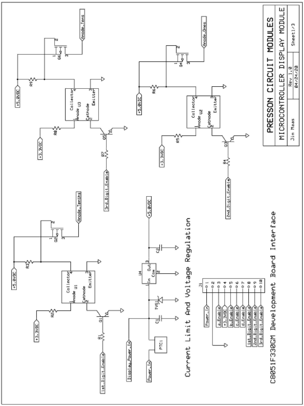
Microcontroller Display Module Schematic Diagrams, cont.
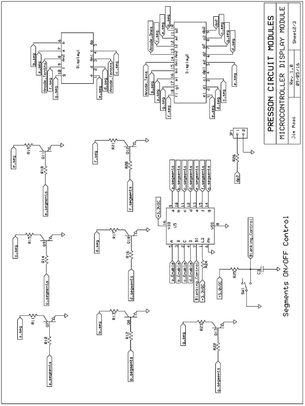
Microcontroller Display Module Schematic Diagrams, cont.:
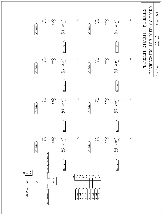
Appendix 2 #
| Table 3 – Microcontroller Display Module Bill of Materials | ||
|---|---|---|
| Component | Description | Product Number |
| C1 | 0.33uF 50V 10% X7R MLCC | 810-FK24X7R1H334K |
| C2 | 0.47uF 50V 10% X7R MLCC | 810-FG28X7R1H474KRT6 |
| C3 | 0.33uF 50V 10% X7R MLCC | 810-FK24X7R1H334K |
| Display1 | single-digit red seven-segment display | 630-HDSP-5501 |
| Display2 | two-digit red seven-segment display | 630-HDSP-521E |
| J1 | 0.1″ RA 10p JTAG header | 517-2310-5121TG |
| J2 | 2p 0.1″ pin strip header | 571-6404522 |
| J3 | 8p 0.1″ pin strip header | 571-6404528 |
| JP1 | 2p 0.1″ pin strip header | 571-6404522 |
| LED0 | 5mm red diffused (618 nm) 2 mcd | 78-TLLR5401 |
| LED1 | 5mm red diffused (618 nm) 2 mcd | 78-TLLR5401 |
| LED2 | 5mm red diffused (618 nm) 2 mcd | 78-TLLR5401 |
| LED3 | 5mm red diffused (618 nm) 2 mcd | 78-TLLR5401 |
| LED4 | 5mm red diffused (618 nm) 2 mcd | 78-TLLR5401 |
| LED5 | 5mm red diffused (618 nm) 2 mcd | 78-TLLR5401 |
| LED6 | 5mm red diffused (618 nm) 2 mcd | 78-TLLR5401 |
| LED7 | 5mm red diffused (618 nm) 2 mcd | 78-TLLR5401 |
| JP3 | 2p 0.1″ pin strip header | 571-6404522 |
| JP4 | 2p 0.1″ pin strip header | 571-6404522 |
| JP5 | 2p 0.1″ pin strip header | 571-6404522 |
| L1 | 22uH 0.95ohm 10% | 580-11R223C |
| L2 | 22uH 0.95ohm 10% | 580-11R223C |
| PTC1 | PTC Fuse 0.5A hold current 1 A trip current | 650-RXEF050 |
| PTC2 | PTC Fuse 0.5A hold current 1 A trip current | 650-RXEF050 |
| Q1 | npn general-purpose (kinked lead) | 512-2N3904TFR |
| Q2 | -40V -500mA P-channel enhancement | 689-VP0104N3-G |
| Q3 | npn general-purpose (kinked lead) | 512-2N3904TFR |
| Q4 | -40V -500mA P-channel enhancement | 689-VP0104N3-G |
| Q5 | npn general-purpose (kinked lead) | 512-2N3904TFR |
| Q6 | -40V -500mA P-channel enhancement | 689-VP0104N3-G |
| Q7 | npn general-purpose (kinked lead) | 512-2N3904TFR |
| Q8 | npn general-purpose (kinked lead) | 512-2N3904TFR |
| Q9 | npn general-purpose (kinked lead) | 512-2N3904TFR |
| Q10 | npn general-purpose (kinked lead) | 512-2N3904TFR |
| Q11 | npn general-purpose (kinked lead) | 512-2N3904TFR |
| Q12 | npn general-purpose (kinked lead) | 512-2N3904TFR |
| Q13 | npn general-purpose (kinked lead) | 512-2N3904TFR |
| Q14 | MPSA20 npn small signal equivalent | 512-2N3904TFR |
| Q15 | MPSA20 npn small signal equivalent | G19467 |
| Q16 | MPSA20 npn small signal equivalent | G19467 |
| Q17 | MPSA20 npn small signal equivalent | G19467 |
| Q18 | MPSA20 npn small signal equivalent | G19467 |
| Q19 | MPSA20 npn small signal equivalent | G19467 |
| Q20 | MPSA20 npn small signal equivalent | G19467 |
| Q21 | MPSA20 npn small signal equivalent | G19467 |
| R1 | 6.65Kohm 1/8W 1% metal film | 270-6.65K-RC |
| R2 | 536ohm 1/8W 1% metal film | 270-536-RC |
| R3 | 1Kohm 1/8W 1% metal film | 270-1K-RC |
| R4 | 6.65Kohm 1/8W 1% metal film | 270-6.65K-RC |
| R5 | 536ohm 1/8W 1% metal film | 270-536-RC |
| R6 | 1Kohm 1/8W 1% metal film | 270-1K-RC |
| R7 | 6.65Kohm 1/8W 1% metal film | 270-6.65K-RC |
| R8 | 536ohm 1/8W 1% metal film | 270-536-RC |
| R9 | 1Kohm 1/8W 1% metal film | 270-1K-RC |
| R10 | 12.7Kohm 1/8W 1% metal film | 270-12.7K-RC |
| R11 | 12Kohm 1/8W 1% metal film | 270-12K-RC |
| R12 | 12.7Kohm 1/8W 1% metal film | 270-12.7K-RC |
| R13 | 130ohm 1/8W 1% metal film | 270-130-RC |
| R14 | 12.7Kohm 1/8W 1% metal film | 270-12.7K-RC |
| R15 | 130ohm 1/8W 1% metal film | 270-130-RC |
| R16 | 12.7Kohm 1/8W 1% metal film | 270-12.7K-RC |
| R17 | 130ohm 1/8W 1% metal film | 270-130-RC |
| R18 | 12.7Kohm 1/8W 1% metal film | 270-1K-RC |
| R19 | 130ohm 1/8W 1% metal film | 270-130-RC |
| R20 | 12.7Kohm 1/8W 1% metal film | 270-12.7K-RC |
| R21 | 130ohm 1/8W 1% metal film | 270-130-RC |
| R22 | 12.7Kohm 1/8W 1% metal film | 270-12.7K-RC |
| R23 | 130ohm 1/8W 1% metal film | 270-130-RC |
| R24 | 1Kohm 1/8W metal film | 270-1K-RC |
| R25 | 130ohm 1/8W 1% metal film | 270-130-RC |
| R26 | 130ohm 1/8W 1% metal film | 270-130-RC |
| R27 | 90Kohm 1/8W 1% metal film | 270-90K-RC |
| R28 | 1.5Kohm 1/8W 1% metal film | 270-1.5K-RC |
| R29 | 90Kohm 1/8W 1% metal film | 270-90K-RC |
| R30 | 1.5Kohm 1/8W 1% metal film | 270-1.5K-RC |
| R31 | 90Kohm 1/8W 1% metal film | 270-90K-RC |
| R32 | 1.5Kohm 1/8W 1% metal film | 270-1.5K-RC |
| R33 | 90Kohm 1/8W 1% metal film | 270-90K-RC |
| R34 | 1.5Kohm 1/8W 1% metal film | 270-1.5K-RC |
| R35 | 90Kohm 1/8W 1% metal film | 270-90K-RC |
| R36 | 1.5Kohm 1/8W 1% metal film | 270-1.5K-RC |
| R37 | 90Kohm 1/8W 1% metal film | 270-90K-RC |
| R38 | 1.5Kohm 1/8W 1% metal film | 270-1.5K-RC |
| R39 | 90Kohm 1/8W 1% metal film | 270-90K-RC |
| R40 | 1.5Kohm 1/8W 1% metal film | 270-1.5K-RC |
| R41 | 90Kohm 1/8W 1% metal film | 270-90K-RC |
| R42 | 1.5Kohm 1/8W 1% metal film | 270-1.5K-RC |
| DIP1 | 14p DIP socket | 571-4-1571552-2 |
| SW1 | SPDT miniature slide switch | 611-OS102011MS2QN1 |
| TVS1 | 15.3V (working voltage) unidirectional TVS | 512-P6KE18A |
| U1 | Phototransistor optocoupler | 512-FOD817D |
| U2 | Phototransistor optocoupler | 512-FOD817D |
| U3 | Phototransistor optocoupler | 512-FOD817D |
| U4 | +5.0V 500mA linear regulator | 821-TS7805CZ |
| U5 | CMOS BCD to 7-segment decoder/driver | 595-CD74HC4543E |
| MDM_PCB | 4.5″ x 2.3″ two-layer FR-4 epoxy glass PCB | PCMDISP040520 |
Appendix 3 #
| MDM Ancillary Kit Bill of Materials | ||
|---|---|---|
| Designation | Component Description | Supplier Part Number |
| MF_Jumper | 10-piece 5.9-inch, male-to-female jumper set | 932-MIKROE-512 |
| FF_Jumper | 10-piece, 5.9-inch, female-to-female jumper set | 932-MIKROE-511 |
| 1in_SO_Al | 4-piece 1.0-inch aluminum, hex standoff | 534-2205 |
| 4_40_PH | 4-piece #4-40, 0.25-inch, pan head screw | 534-9600 |
| 4_N_Wash | 4-piece #4 nylon washer | 534-3358 |
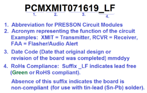
Appendix 4: Anatomy of a PRESSON Circuit Modules PCB Stock Number #
Anatomy of a PRESSON PCB Stock Number
