Downloads #
Introduction #
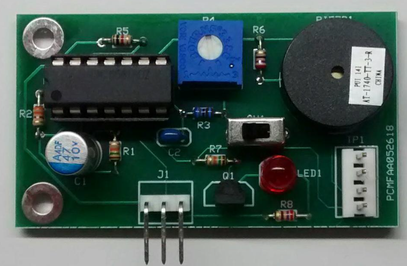
The Flasher/Audio Alert Circuit Module is a compact PRESSON breadboard circuit module featuring two devices: a Renasas/Intersil ICM7556IPDZ dual timer and a 4.0KHz piezo audio transducer. The DigiKey part number for the dual timer contained in a 14-pin dual-inline-package (DIP) is ICM7556IPDZ-ND. (Clicking on this part number will access its DigiKey detail page, which contains a link to the manufacturer’s datasheet. The Mouser Electronics part number for the piezo audio transducer, manufactured by PUI Audio is, 665-AT-1740-TT-3-R. (Clicking this part number will access the Mouser detail page for the product, which contains a link to the manufacturer’s data sheet.) The two timers contained within the ICM7556IPDZ IC are designed to operate independently. On the FAA Breadboard Module, one timer operates as a slow astable multivibrator (a free-running pulse circuit that produces a rectangular waveform). This first timer has an operating frequency of 1.0Hz and a duty cycle (δ) of nearly 50%. The second timer operates as a fast astable multivibrator. Its circuitry contains a single-turn 20KΩ trimmer resistor that allows adjustment of its operating frequency to 4.0KHz, the resonant frequency of the piezo audio transducer. The output of the slow timer serves as the enabling signal for the second timer. While the slow timer’s output signal is high, the second time is enabled to produce its 4.0KHz audio excitation signal. Also, during the duty cycle of the slow timer, a transistor switch turns on, illuminating a bright red LED. A miniature single-pole/double-throw (SPDT) slide switch allows disabling of the audio signal while the LED continues to flash.
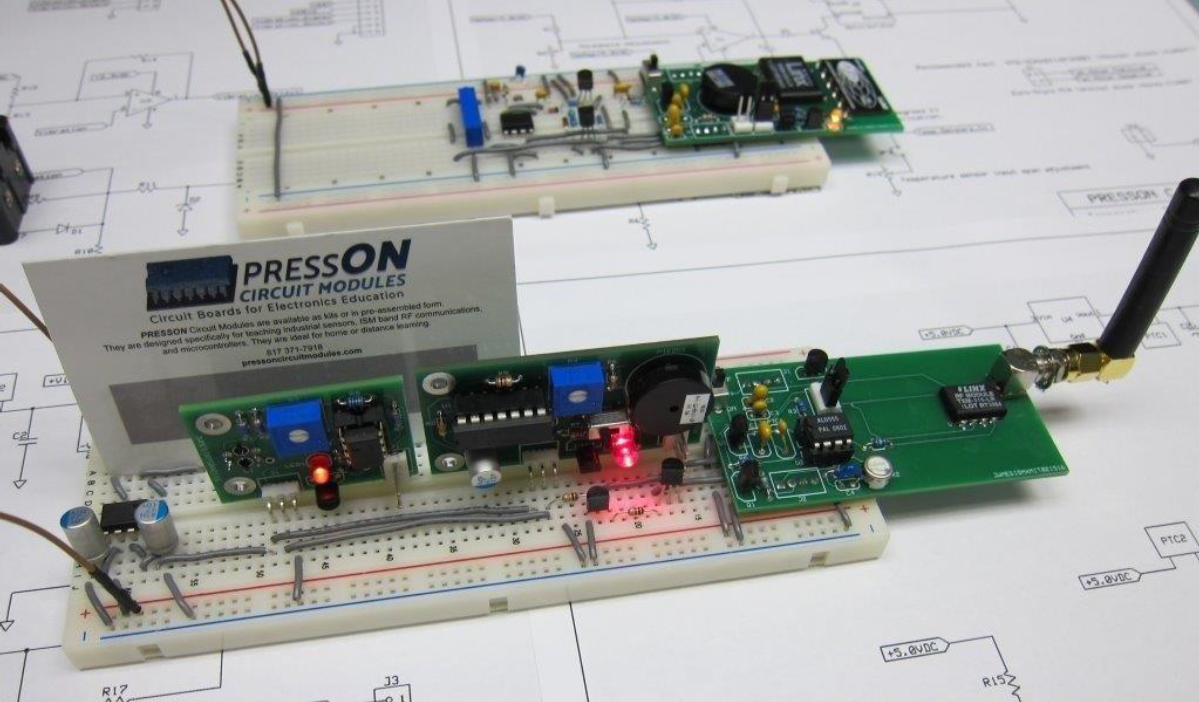
The FAA Breadboard Module is designed specifically for student experimentation, with a three-position right-angled pin header that allows easy vertical insertion into a student’s breadboard. A four-position straight pin header provides two test points, allowing easy connection to an oscilloscope for observation of the fast and slow astable signals. The FAA Breadboard Module is used frequently in the experimental procedures found within the PCM eLearning courseware. An introductory exercise provides a brief theory of operation for the board and contains instructions for testing its operation. A second experiment involves the operation of the FAA Breadboard Module in conjunction with the PRESSON Reflective Proximity Sensor Module. A third laboratory exercise, in the form of a capstone project, involves the operation of the FAA Breadboard Module, the Reflective Proximity Sensor Module, and the PRESSON Simple 315MHz Transmitter and Receiver Modules. The FAA Breadboard Module is available in assembled or unassembled kit form. Figure 1 shows a possible connection of the breadboard modules in development of a capstone project.
Printed Circuit Board Specifications #
The FAA Breadboard Module is contained on a two-sided FR-4 epoxy glass printed circuit board with 1/2-ounce copper laminate. The board dimensions are 2.3″ x 1.3.” The lower layer of the board contains a ground plane, with two grounded 0.125″ mounting holes located at its left-hand corners. These holes allow for panel mounting of the PCB, with possible chassis grounding to a metal enclosure or base plate using conducive metal PCB standoffs . (Go to the PRESSON Circuit Modules website to view economically priced insulated and non-insulated standoff kits.) Figure 2 shows the upper, or silk screen, layer of the PCB, which clearly indicates the location (land pattern or footprint) of each component.
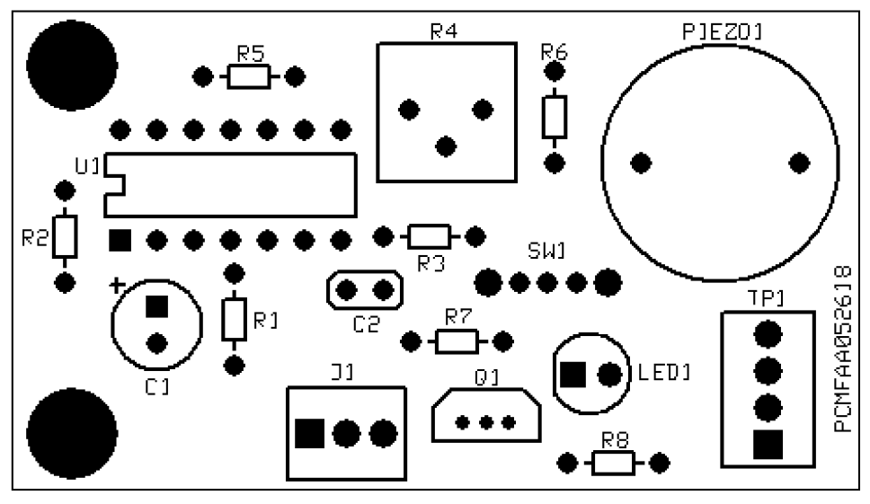
Figure 3 uses colors to represent the three layers of the FAA Breadboard Module. Here, the ground plane and traces on the lower layer of the circuit board are represented in green, while traces and pads on the upper layer of the board are shown in red. Locations of components on the upper (silk-screen) layer of the PCB are shown in yellow.
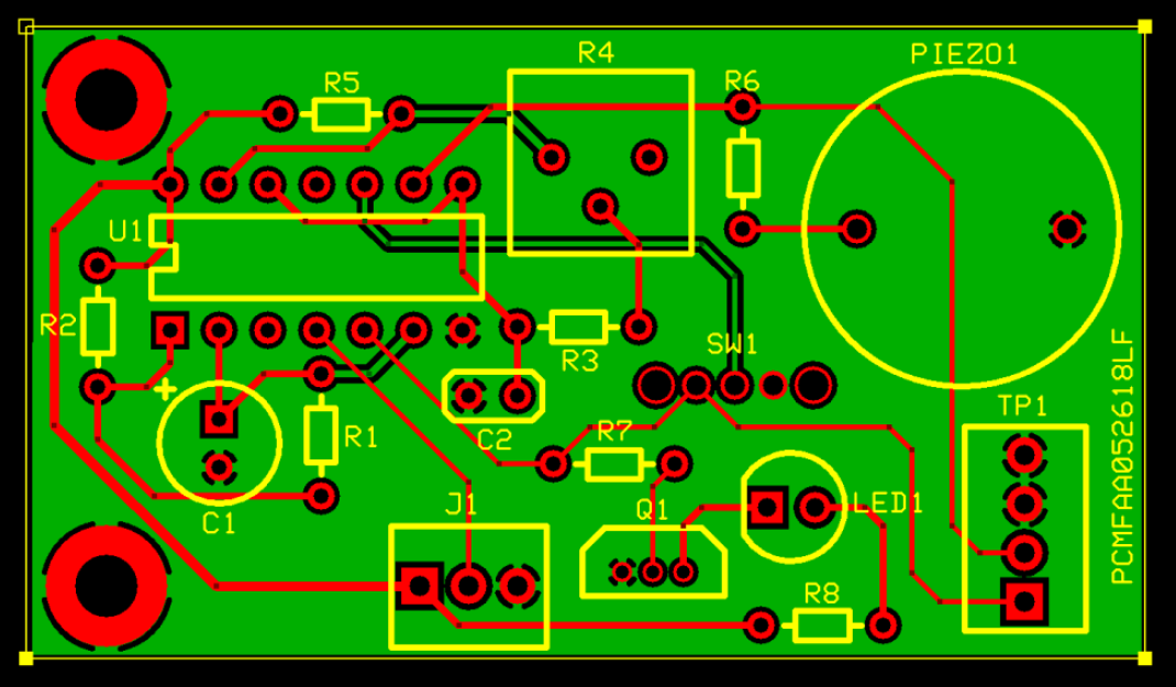
Table 1 lists and defines several of the reference designators used to identify components contained on PRESSON Circuit Modules products.
| Table 1 – Common Component Designators | |
|---|---|
| Designation | Description |
| J (J1, J2, J3…) | Input/Output Connector |
| TP (Tp1, TP2, TP3…) | Test Point |
| JP (JP1, JP2, JP3…) | Jumper Position |
| R (R1, R2, R3…) | Resistor |
| C (C1, C2, C3…) | Capacitor |
| L (L1, L2, L3…) | Inductor |
| U (U1, U2, U3…) | Integrated Circuit (IC) |
| Q (Q1, Q2, Q3…) | Transistor |
| LED (LED1, LED2…) | Light Emitting Diode |
| PTC (PTC1, PTC2…) | Resettable Fuse |
| RT (RT1, RT2, RT3) | Thermistor |
| K (K1, K2, K3…) | PCB Relay |
| SW (SW1, SW2…) | Switch |
Flasher/Audio Alert Board Pin-In and Pin-Out #
Figure 4 shows the pin-in/pin-out of the FAA Breadboard Module. Right-angled, three-position pin header J1 serves as the input/output interface for the FAA Breadboard Module. As seen in Figure 1, this connector allows the module to insert vertically into the user’s breadboard. The module is designed to receive +5.0VDC from the user’s breadboard via pin 1 of J1 (the square pad highlighted in orange). Traces that distribute +5.0VDC throughout the module are highlighted in white, while round pads that provide +5.0VDC to the module components are highlighted in orange. Pin 2 of J1, a round pad highlighted in yellow, receives an Enable_Timer signal from control circuitry fabricated on the user’s breadboard. A logic low or ground connection at this pin inhibits operation of dual CMOS timer U1. A logic 1 or an open-circuit condition at this pin allow continuous operation of the U1 timers. Pin 3 of J1 is soldered to a thermal pad connected to the common ground plane on the lower layer of the PCB. Pads connecting to the ground plane layer are highlighted in blue. The two larger thermal pads in the upper and lower left-hand corners of the PCB allow connection of the ground plane layer of the module to the chassis ground of a larger electronic control system. This connection can be made using hardware contained in the PRESSON Non-Insulated Standoff Kit.

Test point TP1 is a four-position pin-strip header that serves as a convenient connection point for user test equipment. Pin 1 of TP1, the square pad highlighted in yellow, provides access to the Audio_Enable signal, a 1Hz square wave provided by timer 1 of U1. Pin 2 of TP1, the round pad highlighted in yellow, provides access to the Audio_Alert signal, a 4.0KHz rectangular wave used to drive audio transducer PIEZO1. Pins 3 and 4 of TP1 serve as test equipment ground connection points. Figure 5 shows the recommended method for connecting test equipment to the test points on a circuit module. Using jumper leads as shown here prevents “wear and tear” on the test point header pins.

Flasher/Audio Alert Module Operation #
The active component of the FAA Breadboard Module is the ICM7556IPDZ dual timer U1, which contains two independently operating 555 timers. Both timers within the IC are configured to operate as astable, or free running, multivibrators. Figure 6 contains the schematic diagram of the slow 555 timer stage, which is configured to oscillate at nearly 1.0Hz.
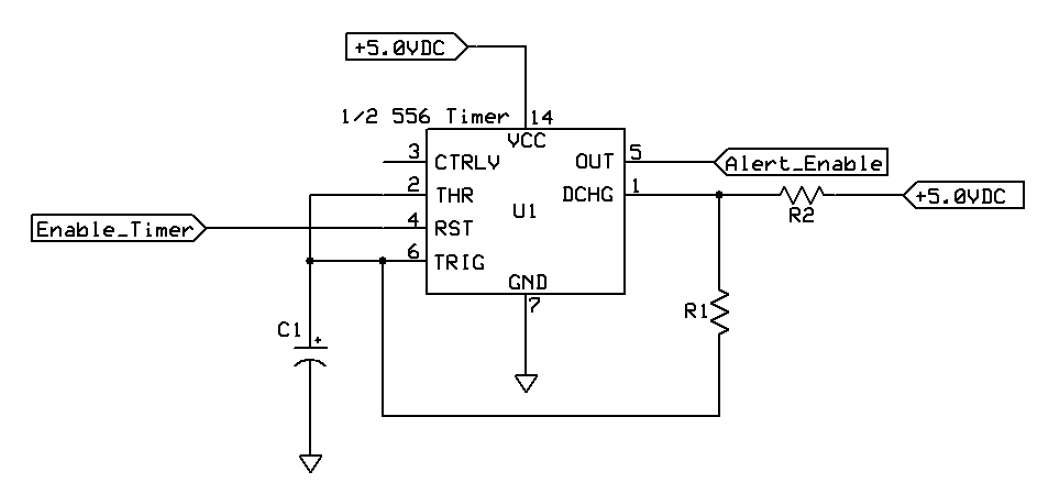
For the slow 555 timer stage, the pulse width (PW) is the time in which the Alert_Enable signal at pin 5 of U1 is at a logic high. Pin 5 holds at a logic high while capacitor C1 charges via R1 and R2 which, during charge time, are effectively in series. When capacitor C1 attains a voltage level of nearly 2/3 the supply voltage (+3.33VDC), the voltage at pin 5 falls low and the capacitor begins to discharge via R1. The pulse width duration is determined as shown by Equation 1. This calculation is based on the assumption that the slow timer has been running for several cycles and the lower threshold for capacitor voltage has stabilized at approximately 1/3 of the supply voltage (+1.67VDC).
Equation 1
During the space width (SW) of the signal at pin 5 of U1, the Alert_Enable signal is at a logic low. While pin 5 is low, C1 discharges into pin 1 of U1 via resistor R1. Pin 5 of U1 holds at a logic low until the capacitor voltage decreases to about +1.67VDC. At that instant, Pin 5 toggles to a logic high, initiating the next cycle of the Alert_Enable signal. The space width of the Alert_Enable signal is determined as shown by Equation 2. (Component values are specified in Appendix 1.)
Equation 2
The period of the Alert_Enable signal (T) is equivalent to PW + SW, while the frequency of that signal is the reciprocal of the period. As shown in Equation 3:
Equation 3
The Alert_Enable signal at pin 5 of U1 controls the operation of the 4.0KHz timer section of U1. As illustrated in Figure 7, actuating single-pole/double-throw (SPDT) slide switch SW1 to the left-hand position provides continuity between pins 5 and 10 of U1.
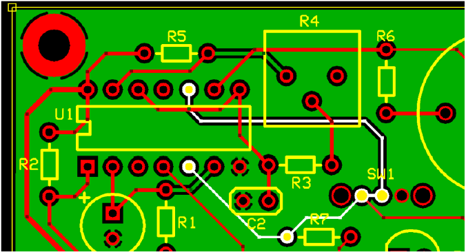
With SW1 actuated to the left, the Alert_Enable signal becomes the Audio_Enable for the fast timer circuitry of U1, which can be adjusted to produce a 4.0KHz audio excitation signal. As shown in Figure 8, the Audio_Enable signal functions as the Reset (RST) input to the second 555 timer. Thus, when the Alert_Enable signal is low, the second 555 timer is held in a reset condition, inhibiting its 4.0KHz output signal. With the Alert_Enable signal at a logic high, the Reset input to the second 555 timer is also high, allowing production of its 4.0KHz output signal. Note that actuating SW1 to the right-hand position breaks the continuity between pins 5 and 10 of U1 and holds pin 10 of U1at ground potential (0.0 volts). Thus, the second 555 timer is held in a continuous reset state, inhibiting production of the audio excitation signal.
As seen in Figure 8, trimmer resistor R4 is located in both the charge and discharge path for capacitor C2. By adjusting the wiper of trimmer potentiometer R4, the user can set the Audio_Alert signal to 4.0KHz, the resonant frequency of audio transducer PIEZO1.
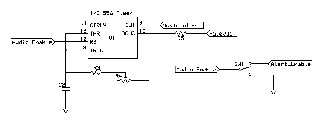
For any given setting of R4, the pulse width and space width of the Audio_Alert signal are determined as shown by Equations 4 and 5.
Equation 4
Equation 5
Note that in Figure 9, the actuator of trimmer resistor R4 is set nearly at its midpoint. With this condition, the resistance between the wiper and either end terminal of R4 should equal approximately 10KΩ. Thus, with R4 connected as shown in Figure 8, R3 + R4 + R5 will equal nearly 6.8KΩ + 10KΩ + 1KΩ. Inserting these values in equations 4 and 5:
With the actuator of R4 already near its midpoint, it could be turned slightly CW or CCW as necessary to obtain the clearest tone while PIEZO1is sounding
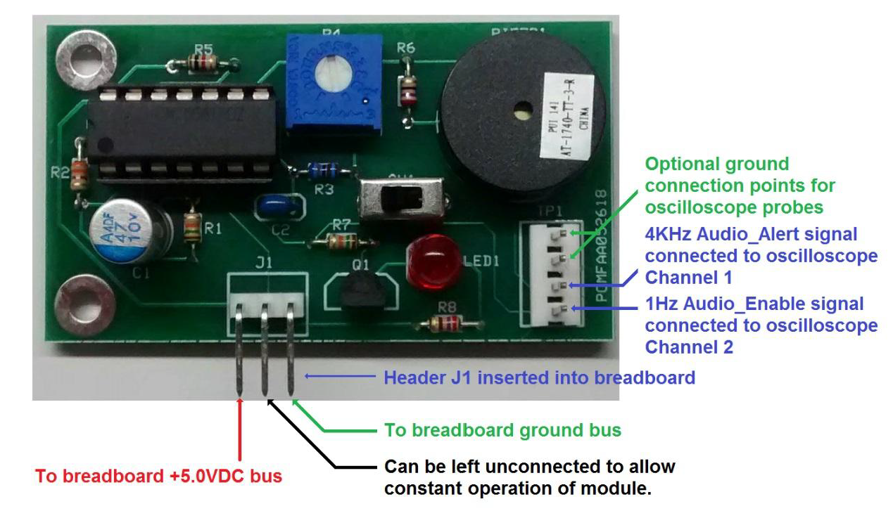
Figure 9 indicates a method for connecting the FAA Breadboard Module to the user’s breadboard and observing the fast and slow 555 timer waveforms. Note that leaving pin 2 of J1 unconnected allows the module to operate continuously. With slide switch SW1 actuated to the left-hand position as shown, PIEZO1 will sound during the 1/2-second high state of the Audio_Enable signal, which can be observed at pin 1 of test point TP1. With these settings, the 4.0KHz audio excitation signal will be present at pin 2 of test point TP1 while the Audio_Enable signal is high.
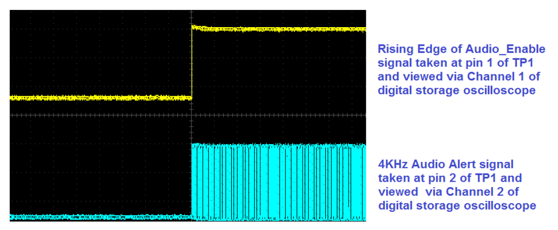
With the oscilloscope adjusted for simultaneous observation of channels 1 and 2 and the probes connected to TP1 as specified in Figure 9, the Audio_Enable and Audio_Alert signals can be observed as shown in Figure 10, with the 4.0KHz audio burst beginning at the rising edge of the Audio_Enable pulse.
The left-hand side of Figure 11 contains the schematic representation of the excitation circuitry for audio transducer PIEZO1. Like a conventional audio speaker, the piezo transducer vibrates in response to an AC signal occurring within the audio frequency range. While a speaker is designed to respond within a specified range of frequencies, a piezoelectric audio transducer is a crystalline device designed to resonate (or produce its strongest output signal) at a specified audio frequency. For the AT-1740-TT-3-R audio transducer, that frequency is 4.0KHz. The graph at the right-hand side of Figure 11 (extracted from the AT-1740-TT-3-R datasheet) contains the frequency response curve of the AT-1740-TT-3-R. Note this device resonates at a peak audio level of nearly 82 dB SPL (decibels of sound pressure level) at an excitation frequency of 4.0KHz.
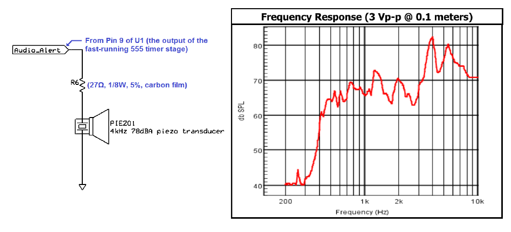
Figure 12 contains a more detailed view of the Audio_Alert signal as seen on a typical digital storage oscilloscope display. To set this signal to the desired excitation frequency of 4.0KHz, the user would adjust the wiper of trimmer resistor R4 using a non-metallic screw driver or alignment tool. Increasing the resistance of R4 lowers the frequency of the Audio_Alert signal, while decreasing R4 resistance increases the signal frequency. The pitch of the audio signal goes lower as the frequency of the astable excitation signal is decreased and goes higher as frequency is increased. As frequency is brought closer to the resonant level of 4.0KHz, the user should notice an increase in clarity and signal strength for the audio output of PIEZO1.

Figure 13 contains the schematic representation of the driver circuitry for LED1, a superbright red 5mm LED indicator. Here, Q1 functions as a buffer, or current-amplifying transistor switch for the LED indicator. In the common emitter configuration shown here, a relatively small amount of base current, drawn from pin 5 of U1, produces a relatively large amount of collector current, adequate for bright illumination of the LED.
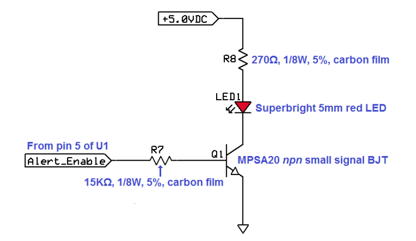
Equation 6 shows the approximation of base current (IB) for transistor Q1. Here the logic high level of the Alert_Enable signal (VIN) is assumed to equal +4.5V and the base-to-emitter forward voltage drop for the transistor switch (VBE) is assumed to be 0.7V. Also, RB in this equation is equivalent to R7 in Figure 13.
Equation 6
Collector current for transistor Q1 can be approximated as shown in Equation 7, where RC is equivalent to R8 in Figure 13.
Equation 7
Per the MPSA20 datasheet the minimal DC current gain (HFE) for transistor Q1 in Figure 13 is 40. As indicated in Equation 8, this current gain is the ratio of collector current to base current.
Equation 8
While using Equation 7 to determine the collector current flow through LED1, we assumed that transistor Q1 was in a saturated condition. This is a safe assumption considering the actual ratio of collector (11.5mA/253μA) is only 45.5. As specified in the datasheet for the MPSA20 transistor, DC current gain can range from 40 to 400. So, the actual hFE for Q1 in Figure 13 is likely to be much higher than 45.5.
Appendix 1 #
The following is a complete listing of components comprising the PRESSON Flasher/Audio Alert Breadboard Module. With the exception of the PCMFAA052618 PCB, replacement parts for the module can be ordered from Mouser Electronics. The blank PCB can be ordered from PRESSON Circuit Modules, Inc.
| Table 2 – Bill of Materials | ||
|---|---|---|
| Component | Description | Product Number |
| C1 | 47uF 10V 20% organic polymer | 661-PSA10VB47M |
| C2 | 0.01uF 50V C0G 5% MLCC | 594-K103K15X7RF53L2 |
| J1 | 3p 0.1″ right angle header | 538-22-05-2031 |
| LED1 | 5mm (T-1 3/4) red (635 nm) | MPJA 15108 OP |
| PIEZO1 | 4kHz 78dBA piezo transducer | 665-AT-1740-TT-3-R |
| Q1 | MPSA20 npn small signal equivalent | G19467 |
| R1 | 15Kohm 1/8W 5% carbon film | 299-15K-RC |
| R2 | 330ohm 1/8W 5% carbon film | 299-330-RC |
| R3 | 6.8Kohm 1/8W 5% carbon film | 299-6.8K-RC |
| R4 | 20Kohm 1/2W 10% single-turn trimmer | 652-3386P-1-203LF |
| R5 | 1Kohm 1/8W 5% carbon film | 299-1K-RC |
| R6 | 27ohm 1/8W 6% carbon film | 299-27-RC |
| R7 | 7.5Kohm 1/8W 5% carbon film | 299-7.5K-RC |
| R8 | 130ohm 1/8W 5% carbon film | 299-130-RC |
| SW1 | SPDT slide switch | 611-0S102011MS2QN1 |
| TP1 | 4p 0.1″ pin strip header | 517-929705-01-04-EU |
| U1 | Dual CMOS Precision Timer | 968-ICM7556IPDZ |
| DIP14 | 14p dual-wipe dip socket | 517-4814-3004-CP |
| FAA_PCB | Reflective Photosensor Module PCB | PCMFAA052618 |
Appendix 2 #
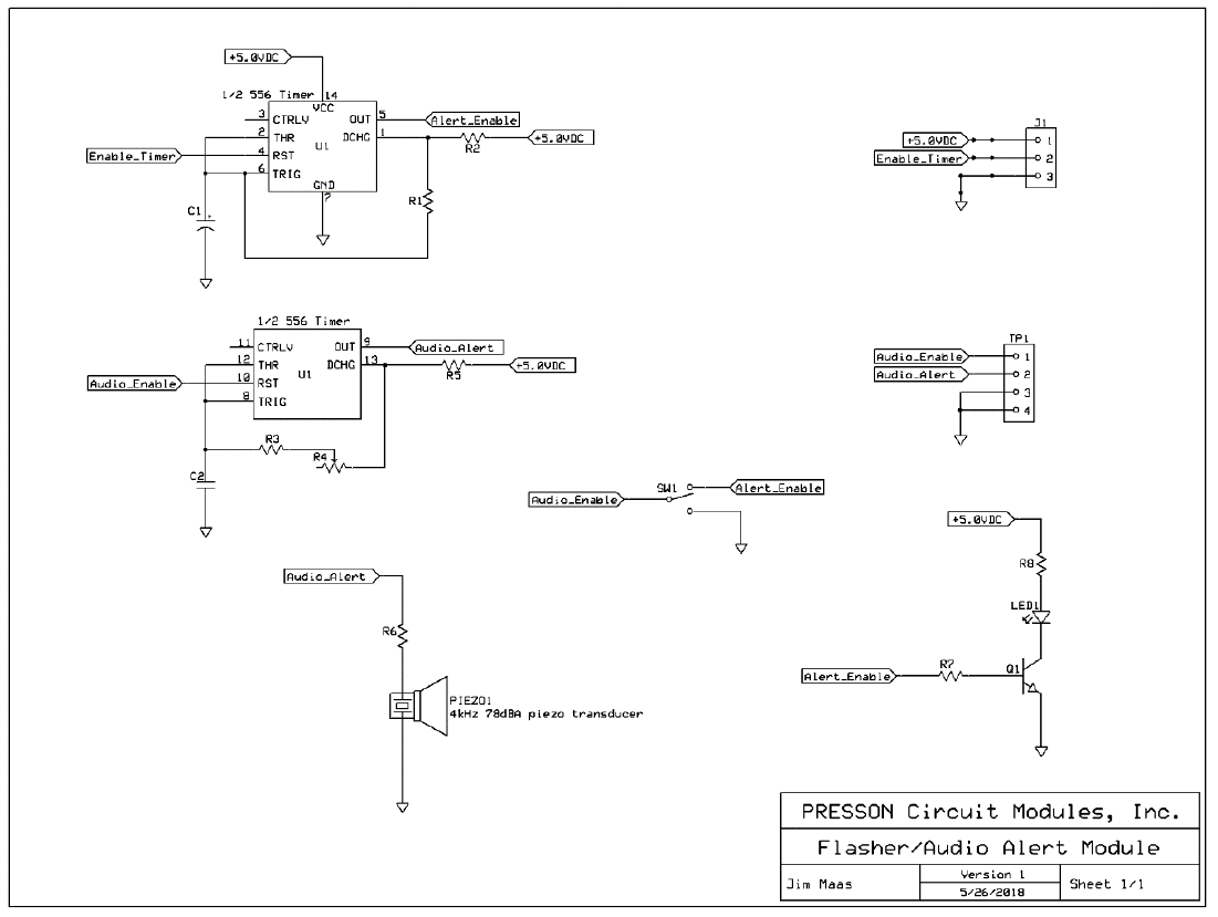
Figure 14 contains the complete schematic diagram of the circuitry comprising the PRESSON Flasher/Audio Alert Breadboard Module.
Appendix 3 #
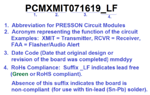
Anatomy of a PRESSON PCB Stock Number
