Downloads #
Introduction #

The PRESSON DC Voltage Breakout Module is a free-standing circuit board designed to function as a convenient source for DC voltages commonly used by low-power circuitry contained within industrial control systems. The module can accept a DC input ranging from +18.0 VDC to nearly +30.0 VDC and extract four highly regulated output voltage channels consisting of +3.3VDC, +5.0VDC, +9.0VDC, and +12.0VDC. It can also accept a +12.0VDC input from an external power source and provide the +3.3VDC, +5.0VDC, +9.0VDC output channels. In either operating configuration, the module provides a daisy chain output for its input voltage. The primary purpose of the module is to expedite lab experimentation by significantly reducing the time and materials required to fabricate circuitry on a breadboard where multiple voltage sources are required.
While the DC Voltage Breakout Circuit Module serves as an important tool for efficient system prototyping, it is also serves as a focal point for hands-on lab experimentation during the Introduction to Industrial DC Power Sources course contained in Track Five of the PRESSON Circuit Modules curriculum. The module serves as a platform for the study of linear bandgap voltage regulators, DC/DC switching voltage regulators, and a low-dropout PMOS voltage regulator. This circuit module is also available in kit form and can be easily assembled by a student possessing intermediate level soldering skills.
Printed Circuit Board Specifications: #
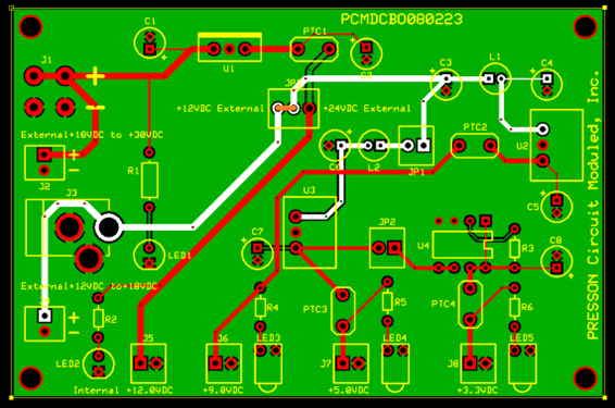
The PRESSON DC Voltage Breakout Circuit Module is contained on a two-layer FR-4 epoxy glass PCB (printed circuit board) with 1/2 oz copper laminate. The board dimensions are 3.8″ x 2.5.” The lower layer of the board contains a common ground plane, with grounded 0.125″ mounting holes in the four corners. These holes allow for panel mounting of the PCB to a grounded chassis or base plate. Figure 1 shows the silk-screening on the upper layer of the PCB, clearly indicating the location of each component.
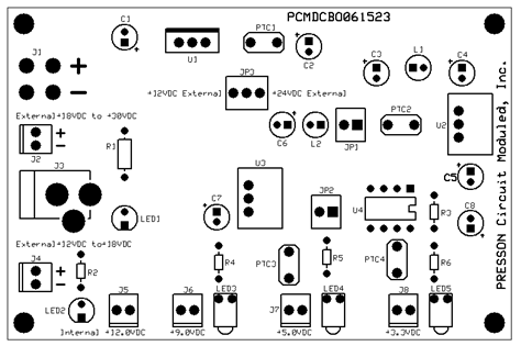
Figure 2 uses colors to represent the two sides of the DC Voltage Breakout Module. Here, the ground plane and traces on the lower side of the circuit board are represented in green, while traces, pads, and vias on the upper sider are shown in red. The locations of components on the upper, silk screen layer of the PCB are shown in yellow.
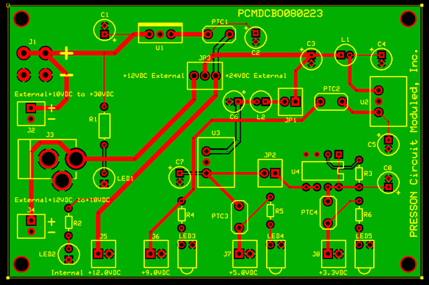
Table 1 identifies and defines several of the reference designators commonly used to represent components contained on PRESSON Circuit Modules products.
| Table 1 – Common Component Designators | |
|---|---|
| Designation | Description |
| J (J1, J2, J3…) | Input/Output Connector |
| TP (Tp1, TP2, TP3…) | Test Point |
| JP (JP1, JP2, JP3…) | Jumper Position |
| R (R1, R2, R3…) | Resistor |
| C (C1, C2, C3…) | Capacitor |
| L (L1, L2, L3…) | Inductor |
| U (U1, U2, U3…) | Integrated Circuit (IC) |
| Q (Q1, Q2, Q3…) | Transistor |
| LED (LED1, LED2…) | Light Emitting Diode |
| PTC (PTC1, PTC2…) | Resettable Fuse |
| RT (RT1, RT2, RT3) | Thermistor |
| K (K1, K2, K3…) | PCB Relay |
| SW (SW1, SW2…) | Switch |
PRESSON DC Voltage Breakout Module Input/Output Voltage Control: #
Figure 3 illustrates circuit conditions that could exist when the +18VDC to +30VDC input is being utilized as the power source for the DC Voltage Breakout Circuit Module. Here various colors are used to indicate possible paths for the current flow. As indicated by the PCB traces highlighted in white, either header J1 or J2 could serve as the External +18VDC to +30VDC input. If J1 becomes the power source for the module, pin strip header J2 can become a convenient daisy chaining output, allowing the source voltage to be routed to another circuit module or breadboard. Header J2 can also serve as a safe point to monitor the source voltage using a digital multimeter. J1 is a two-position, 0.25″ vertical Quick Fit header manufactured by Keystone Electronics (Mouser part number 534-7832 or Digi-Key part number 36-7832-ND). This component has been selected with the assumption that the breakout board could be permanently installed within a larger electronic control system, where it could receive power from a +24.0VDC power supply embedded within that system. Industrial power distribution systems often contain cabling with female quick disconnect terminals that could fit securely over header J1.
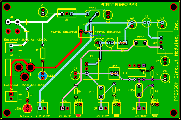
As shown in the upper LH section of Figure 3, headers J1 and J2 connect directly to pin 1 of U1, which is a +12.0VDC linear bandgap voltage regulator manufactured by STMicroelectronics (Mouser part number 511-L7812ABV-DG or Digi-Key part number 497-13138-ND). C1 and C2 are 10µF aluminum organic polymer capacitors. C1 provides noise filtering and stabilization for the input to voltage regulator U1. C2 provides further stabilization of the regulator output.
PTC1 is a resettable fuse, also referred to as a polyswitch. (PTC is the abbreviation for positive temperature coefficient.) A component exhibiting a positive temperature coefficient becomes increasingly resistive as its temperature increases. A polyswitch is characterized by a very abrupt positive temperature coefficient. Providing the current flow through the device remains at or below its holding current level (IH), its resistance remains quite low, typically a fraction of an ohm. However, as current increases toward a maximum allowable level, specified as the trip current (IT), the resistance of the device rapidly increases to a very high ohmic level, virtually inhibiting any further current flow through the device. PTC1 is a Littelfuse polyswitch (part number RHEF070). The holding current for that device is 700mA, while its trip current is 1.4A.
The RUEF070 polyswitch (Mouser part number 650-RHEF070-2) is an ideal choice for protection of linear voltage regulator U1. From the L7812ABV-DG datasheet, we can surmise the maximum allowable continuous output current for that device is 1.5A. While the datasheet describes the regulator as having thermal overload protection, short circuit protection, and internal limiting of output current (IO), PTC1 prevents the regulator’s output current from attaining and holding at its maximum allowable level. Once a resettable fuse trips, power must be removed from the circuitry containing it. The fault causing the over current condition must be remedied before the device can return to and remain in its low resistance state.
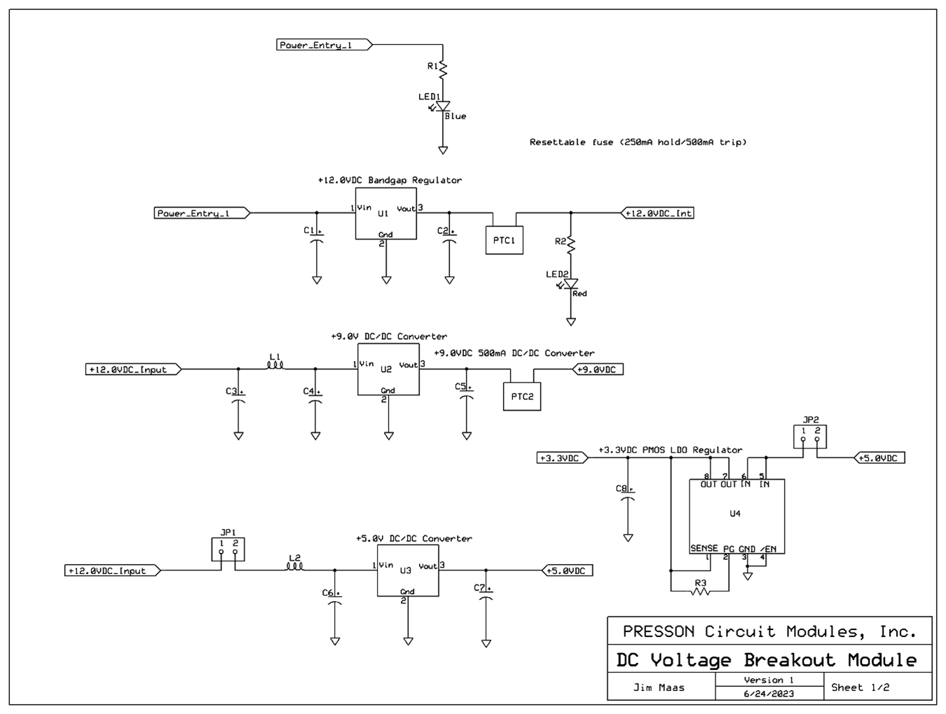
Referring to Figure 3 and the schematic diagram in Figure 4, note that current entering the module via header J1 or J2, flows through ballast resistor R1, illuminating blue indicator LED1, the cathode of which connects to circuit ground. Also, with +18.0 VDC to +30.0VDC present at pin 1 of voltage regulator U1, +12.0VDC will be present at pin 3 of that device. With PTC1 in its low resistance state (around 0.25Ω) +12.0VDC will be present at output header J5 and the +12.0VDC indicator LED2 will illuminate.
Also, with the shunt connected between pins 2 and 3 of JP3, +9.0VDC will be present at pin 1 of U2, which is a DC/DC Converter manufactured by RECOM (part number R-78E9.0-0.5). DC/DC power converters are much more power efficient than linear regulators but they are also more complex. The device contains high frequency inductive/capacitive switching circuitry and, for this reason, could also by described as a switching voltage regulator. The +9.0VDC output present at pin 3 of U2 is present at pin 1 of header J6. (The traces for this output path are highlighted in pink.) Red indicator LED3 illuminates when the +9.0VDC output is enabled. Resettable fuse PTC2 (Littelfuse part number RXEF025) is placed in series between pin3 of U2 and header J6, protecting the regulator from an excessive output current demand. Viewing the datasheet of the R-78E9.0-0.5 regulator, we can surmise maximum allowable output current to equal 500mA, which is the rated value of IT for PTC2. (IH for that device is 250mA.)
Because of their internal switching regulators, DC/DC power converters produce electromagnetic interference (EMI) within contiguous circuitry. Thus, RECOM recommends that low pass filter circuitry be placed at both the input and output of a switching regulator. Inductor L1 and capacitors C3 and C4 form a pi filter, which suppresses any EMI emanating from the input of U2. This filter circuitry is recommended in the R-78E-1.0 series datasheet for meeting the EN55032 EMC standard for inhibiting electromagnetic interference in audio/visual equipment. (EMC is the abbreviation for electromagnetic compatibility.)
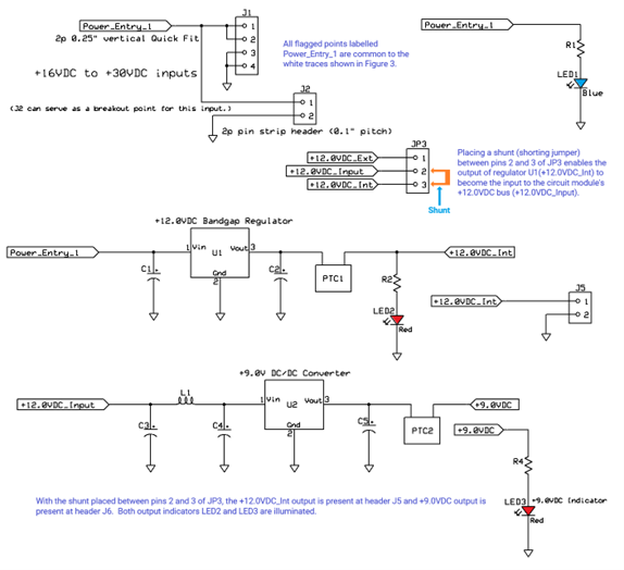
Referring to Figures 3 and 5, note that a branch of the +12.0VDC_Input begins at the positive electrode of capacitor C3. This second path for the +12.0VDC internal bus extends through Jumper position JP1 and inductor L2, terminating at pin 1 of U3. C3, C6 and inductor L2 together form a pi filter, inhibiting EMI emanating from U2 or U3. U3 (RECOM R-78E5.0-0.5) is a +5.0 VDC power converter similar in structure to U2. In Figure 3, the path for output current from that device is indicated in light purple. Like the R-78E9.0-0.5 used in the U2 position, U3 is also assumed to have a maximum output current of 500mA. For this reason, the RXEF025 resettable fuse, serving as PTC3, is placed in series with the output of U3. Assuming PTC3 has not tripped, the +5.0VDC output for the circuit module is available at pin 1 of header J7. Yellow indicator LED3 illuminates when the +5.0VDC output is enabled. Note that, without a shunt inserted over JP1, U3 is effectively removed from the breakout module circuitry.
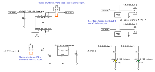
Note that, while providing a +5.0VDC output at J7, U3 also becomes the power source for +3.3VDC regulator U4 (Texas Instruments part number TPS7233QP). The datasheet for the TPS7233QP describes the device as being a low-dropout (LDO), micropower regulator. Per the datasheet for the TPS7233QP, its dropout voltage is specified as 85mV. A linear regulator’s dropout voltage can be easily misunderstood. It is not the lowest input voltage that will work for the given device. (The input voltage to a linear regulator must always be higher than its rated output.) Rather, the regulator’s dropout voltage is the smallest allowable difference between the output of the regulator’s power source and the input to the device. Based on the parameters specified in the datasheet of the TPS7233QP, we could assume the input voltage to the device could be as low as +3.385V and its output would hold at nearly +3.3VDC assuming the output current demand to be no more than 100mA. Describing the device as micropower implies the TPS7233QP is very efficient, dissipating very little power for its own operation. Thus, the TPS72 family of voltage regulators is ideal for use in battery-powered devices. (The TPS7233QP and related products are examined in detail in Track Five of the PCM curriculum.)
Because of its high efficiency, the TPS7233QP can pass up to 1.5A of output current to its load. However, for this application PTC4 (Littelfuse RXEF017) limits the output current of U4 to 340mA. This current limit is imposed with the assumption that any +3,3VDC loads served by the DC Voltage Breakout Circuit Module will be low-power devices such as microcontroller and wireless communication circuitry.
Assume the user only has need of a +12VDC power source for a project but still needs access to the +3.3VDC, +5.0VDC, and +9.0VDC outputs provided by the DC Voltage Breakout Circuit Module. They have the option of connecting power to the module and inserting a shunt over pins 1 and 2 of JP3 as shown in Figure 6. Here, J4 is a two-position pin strip header identical to J2. J3 is a 2.0mm/5.5mm DC Jack (Kycon part number KLDX-0202-A-LT). A recommended connection method for a +12VDC source would be to plug a +12VDC AC adapter with a 2mm center-positive connector to J3, allowing header J4 to serve as a daisy chaining output for the +12VDC input.
As indicated by the traces highlighted in white in Figure 6, with an input taken at either J3 or J4, +12.0VDC regulator U1 is effectively removed from the module’s output control circuitry.
Conclusion: #
The purpose of this document is to provide a general overview of the structure and operation of the PRESSON DC Voltage Breakout Circuit Module. The module is used during lab experimentation within Track Five of the PCM courseware. Here, basic forms of DC power source are examined in detail. U1 is used to investigate the operating parameters of the bandgap family of linear voltage regulators. U2 and U3 are utilized in the study of DC/DC power converters and switching voltage regulators. U4 is used in the study of high-efficiency low-dropout (LDO) linear regulators.
While taking courses contained in the PRESSON eLearning Curriculum, students are strongly encouraged to use the DC Voltage Breakout Circuit Module in lab experimentation and project development. The module will prove to be an invaluable tool in prototyping circuitry that requires multiple voltage sources: +3.3VDC for powering MCU circuitry, +5.0VDC for implementing TTL circuitry, +9.0VDC for development of hand-held/battery-powered devices, and +12.0VDC for working with low-power motor control applications. Use of the DC Voltage Breakout Circuit Module significantly reduces the time and costs involved in developing the aforementioned types of electronic circuitry.
Appendix 1 #
The following is a complete listing of components comprising the DC Voltage Breakout Circuit Module. With the exception of the DCV_BO_PCB (PCMDCBO080223_LF) PCB, replacement parts for the module can be ordered from Mouser Electronics or Digi-Key. The bare PCB can be ordered from PRESSON Circuit Modules, Inc.
NOTE: The bare PCB specified above is RoHS compliant, designed for assembly using lead free solder.
| Table 3 – Microcontroller Display Module Bill of Materials | ||
|---|---|---|
| Component | Description | Product Number |
| C1 | 10uF 50V 20% Aluminum Organic Polymer | 80-A759BQ106M1HAE105 (Digi-Key: 399-A759BQ106M1HAAE105-ND) |
| C2 | 10uF 25V 20% Aluminum Organic Polymer | 80-A758BG106M1EAAE70 (Digi-Key: 399-A758BG106M1EAAE070-ND)) |
| C3 | 10uF 25V 20% Aluminum Organic Polymer | 80-A758BG106M1EAAE70 (Digi-Key: 399-A758BG106M1EAAE070-ND) |
| C4 | 10uF 25V 20% Aluminum Organic Polymer | 80-A758BG106M1EAAE70 (Digi-Key: 399-A758BG106M1EAAE070-ND) |
| C5 | 10uF 25V 20% Aluminum Organic Polymer | 80-A758BG106M1EAAE70 (Digi-Key: 399-A758BG106M1EAAE070-ND) |
| C6 | 10uF 25V 20% Aluminum Organic Polymer | 80-A758BG106M1EAAE70 (Digi-Key: 399-A758BG106M1EAAE070-ND) |
| C7 | 10uF 25V 20% Aluminum Organic Polymer | 80-A758BG106M1EAAE70 (Digi-Key: 399-A758BG106M1EAAE070-ND) |
| C8 | 10uF 25V 20% Aluminum Organic Polymer | 80-A758BG106M1EAAE70 (Digi-Key: 399-A758BG106M1EAAE070-ND) |
| J1 | 2p 0.25″ vertical Quick Fit | 534-7832 (Digi-Key: 36-7832-ND) |
| J2 | 2p pin strip header (0.1″ pitch) | 651-1725656 (Digi-Key: 277-5810-ND) |
| J3 | 2.0mm/5.5mm DC Jack | 806-KLDX-0202-A-LT (Digi-Key 2092-KLDX-0202-A-LT-ND) |
| J4 | 2p jack screw terminal block (0.1″ pitch) | 651-1725656 (Digi-Key: 277-1273-ND) |
| J5 | 2p jack screw terminal block (0.1″ pitch) | 651-1725656 (Digi-Key: 277-1273-ND) |
| J6 | 2p jack screw terminal block (0.1″ pitch) | 651-1725656 (Digi-Key: 277-1273-ND) |
| J7 | 2p jack screw terminal block (0.1″ pitch) | 651-1725656 (Digi-Key: 277-1273-ND) |
| J8 | 2p jack screw terminal block (0.1″ pitch) | 651-1725656 (Digi-Key: 277-1273-ND) |
| JP1 | 2p vertical pin strip header (0.1″ pitch) | 571-6404522 (Digi-Key: A1911-ND) |
| JP2 | 2p vertical pin strip header (0.1″ pitch)) | 571-6404522 (Digi-Key: A1911-ND) |
| JP3 | 3p pin strip header (0.1″ pitch) | 571-6404523 |
| L1 | 3.9uH 720mA 300mΩ | 994-RFB0807-3R9L (Digi-Key: RLB0608-3R9ML-ND) |
| L2 | 3.9uH 720mA 300mΩ | 994-RFB0807-3R9L (Digi-Key: RLB0608-3R9ML-ND) |
| LED1 | Low current blue 3mm LED indicator | 604-WP710A10LVBCD (Digi-Key: 754-1914-ND) |
| LED2 | 3mm (T-1) diffused red | 604-WP132XID (Digi-Key: 754-1211-ND) |
| LED3 | 3mm (T-1) diffused red LED assembly | 749-H101CRD (Digi-Key: 492-1874-ND) |
| LED4 | 3mm (T-1) yellow LED assembly | G20820 (Dialight 5510307F) |
| LED5 | 3mm (T-1) green LED assembly | 749-H101CGD (Digi-Key: 492-1873-ND) |
| PTC1 | resettable fuse (700mA hold/1.4A trip) | 650-RHEF070-2 |
| PTC2 | Resettable fuse (250mA hold/500mA trip) | 650-RXEF025 |
| PTC3 | Resettable fuse (250mA hold/500mA trip) | 650-RXEF025) |
| PTC4 | Resettable fuse (170mA hold/340mA trip) | 650-RXEF017 |
| R1 | 4.3Kohm 1/4W 5% carbon film | CF14JT4K30CT-ND (Digi-Key) |
| R2 | 2.2Kohm 1/8W 5% carbon film | 299-2.2K-RC (Digi-Key CF18JT2K20CT-ND) |
| R3 | 249Kohm 1/8W 1% metal film | 270-249K-RC (Digi-Key: CF18JT240KCT-ND) |
| R4 | 680ohm 1/8W 5% carbon film | CF18JT680RCT-ND (Digi-Key) |
| R5 | 270ohm 1/8W 5% carbon film | CF18JT270RTR-ND (Digi-Key) |
| R6 | 82ohm 1/8W 5% carbon film | CF18JT82R0CT-ND (Digi-Key) |
| U1 | +9.0VDC 500mA DC/DC Converter | 511-L7812ABV-DG (Digi-Key: 497-13138-ND) |
| U2 | +9.0VDC 500mA DC/DC Converter | 919-R-78E9.0-0.5 (Digi-Key: 945-2638-5-ND) |
| U3 | +5.0V DC/DC converter | 919-R-78E5.0-0.5 (Dig-Key: 945-1648-5-ND) |
| U4 | +3.3VDC PMOS LDO | 595-TPS7233QP (Digi-Key 296-8056-5-ND) |
| DIP_1 | Dual-leaf ladder-type 8p DIP socket | 571-1-2199298-2 |
| JP1_Shunt | Shunts with handle | 571-8815452 |
| JP2_Shunt | Shunts with handle | 571-8815452 |
| JP2_Shunt | Shunts with handle | 571-8815452 |
| Alu_Standoff_Set | 1/2″ nylon hex standoffs w 4-40 thread (four piece set) | 534-1893 |
| Nylon_Washer_Set | #4 nylon washer (four piece set) | 534-3358 |
| Steel_Screw_Set | #4-40 1/4″ pan head (four piece set) | 534-9300 |
| TO-220_HS_1 | TO-220 heat sink | 532-577002B00 |
| TO_220_HSM_Kit | TO-220 heat sink mounting kit with mica insulator | 532-4880M (Digi-Key: 4880MG-ND) |
| DCV_BO_PCB | 2-layer 2.5″ x 3.8″ PCB with common ground plane, silk screen, and solder mask | PCMDCBO080223 (ExpressPCB number = BDJQ10089N) |
Appendix 2 #
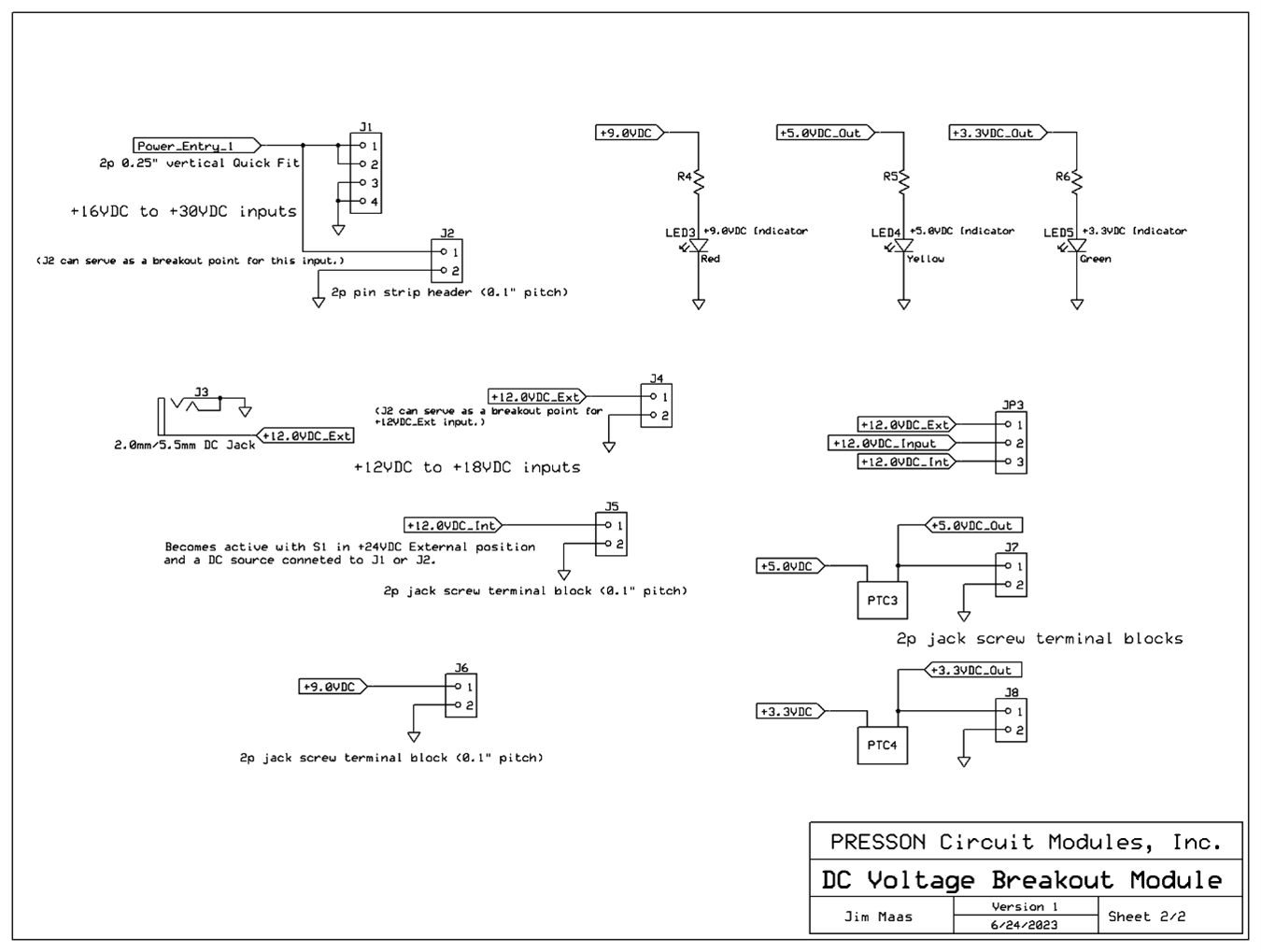
Figures 7 and 8 contain sheets 1 and 2 of the schematic diagrams the PRESSON Simple 315MHz Transmitter Module.
Appendix 3: Anatomy of a PRESSON Circuit Modules PCB Stock Number #
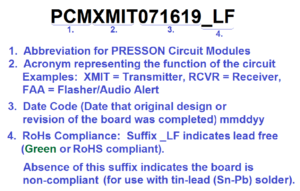
Anatomy of a PRESSON PCB Stock Number
