Downloads #
Introduction #
The Simple 315MHz Transmitter Module and Simple 315MHz Receiver Module together provide a seamless platform for sending discrete control signals or serial data wirelessly over short distances. This complementary transmitter/receiver pair is designed primarily for electronics education, demonstrating the use of wireless technology in everyday applications such as remote control, remote sensing, and keyless access. Containing no encoding/decoding circuitry, these modules provide a seamless serial interface between a transmitting control source and a remote destination. The serial bit stream fed to the data input of the transmitter module is directly demodulated by the receiver. To create a secure simplex communication link between the source and destination, designers must either incorporate encoding/decoding devices into their system or create their own custom protocol through microcontroller programming. The Simple 315MHz transmitter/receiver pair is designed to interface easily with standard encoding/decoding ICs as well as microcontroller input and output ports.
The Linx TXM-315-LR transmitter IC contained on the Simple 315MHz Transmitter Module is designed to modulate its input signal through a technique called on-off keying (OOK), the simplest form of amplitude-shift keying (ASK). Figure 1 contains an example of the of ASK in which the carrier is continuously present. As seen here, the baseband signal, which is modulated by the 315MHz carrier, is a pulsating DC rectangular waveform that rapidly switches between a near zero-volt level and a peak amplitude. For the Simple 315MHz transmitter module, this peak input signal level could vary from around +3.0V to +12.0V. In digital electronics, these high and low signal levels typically represent logic 1 and 0. For the ASK application shown in Figure 1, while the input signal is at a logic high, the 315MHz carrier is at maximum amplitude. While the input signal is at a logic low, the 315MHz carrier is still present, but at a lower amplitude.
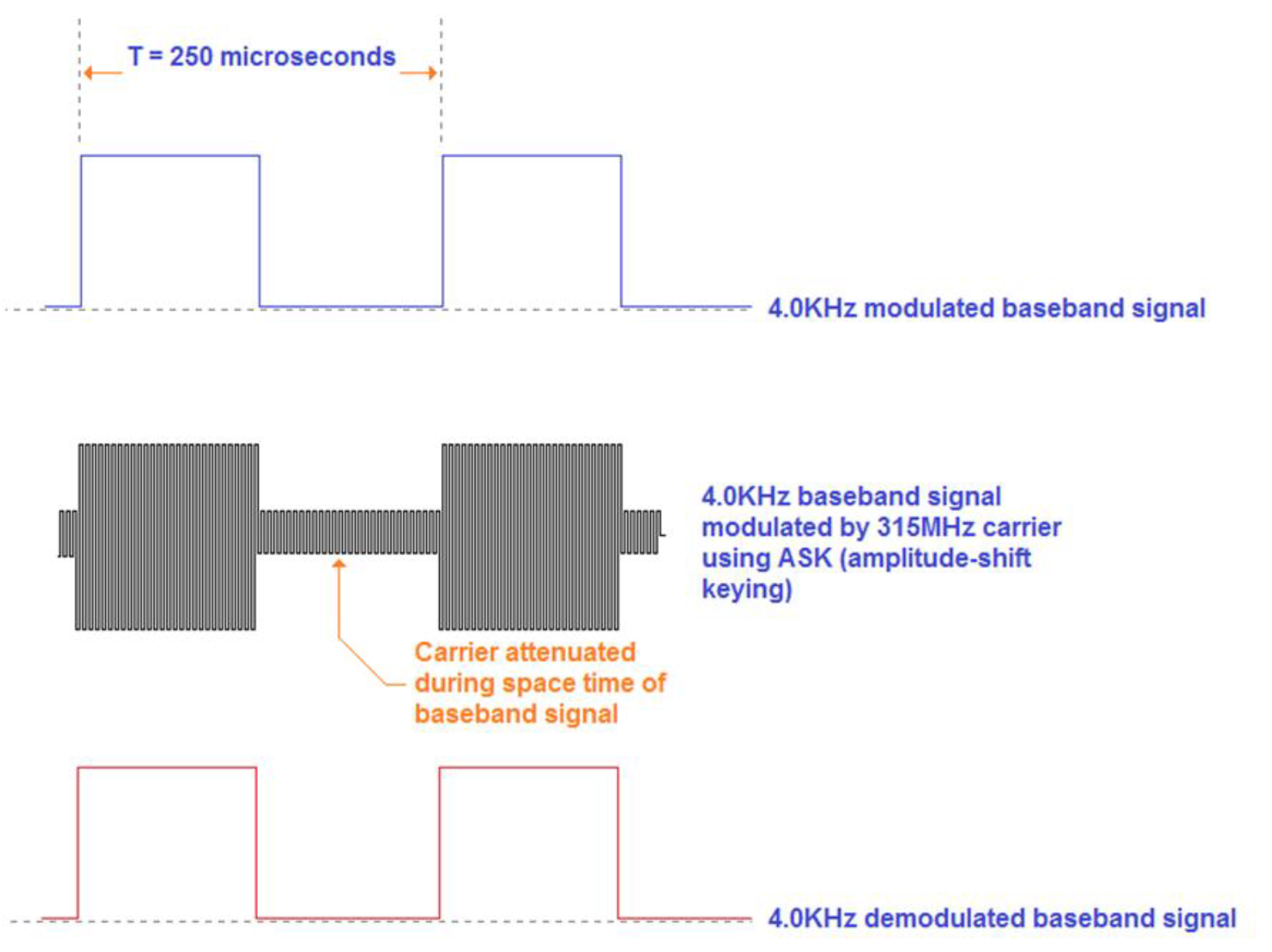
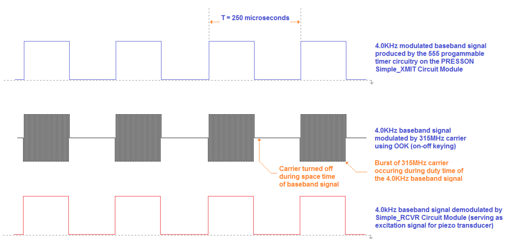
Figure 2 represents OOK, the modulation technique used by the TXM-315-LR transmitter IC on the Simple 315MHz Transmitter Module. Here, as with the example in Figure1, the carrier is at maximum amplitude while the input signal is at a logic high. However, while the input is at a logic zero, the carrier is in an off state. Because the carrier is only present during the high state of the digital input, OOK represents the simplest and most power efficient form of ASK. As indicated by the red rectangular waveforms in Figures 1 and 2, the ASK receiver demodulates the 315MHz carrier, recovering the 4.0KHz rectangular waveform. The RXM-315-LR IC on the on the Simple 315MHz Receiver Module is designed to demodulate the OOK signal transmitted by the TXM-315-LR. The Simple 315MHz Transmitter/Receiver Pair has an important feature that allows easy testing of the transmitter range. As shown in Figure 3, the transmitter module contains a square wave oscillator that can be adjusted to produce a 4.0KHz baseband signal. This signal can be routed to the transmitter input via a jumper connection. At the receiver side, the demodulated 4.0KHz signal can be routed to a piezo audio transducer that resonates at 4.0KHz. With the transmitter module remaining stationary, the user could move the receiver module to a point where the audio signal begins to break up to estimate maximum range. This range checking feature is discussed in detail at a later point in this document.
The Simple 315MHz Transmitter Module Structure and Layout: #
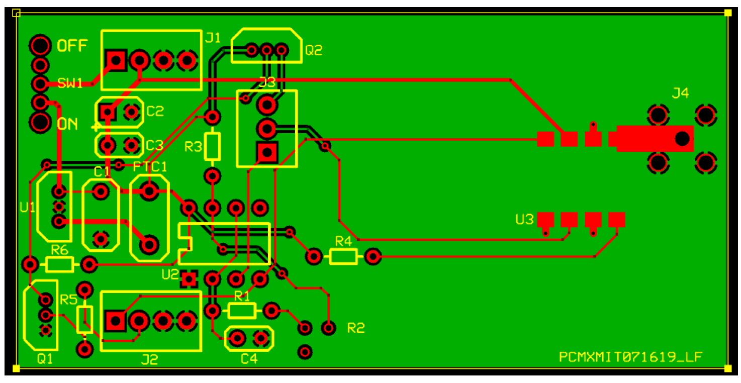
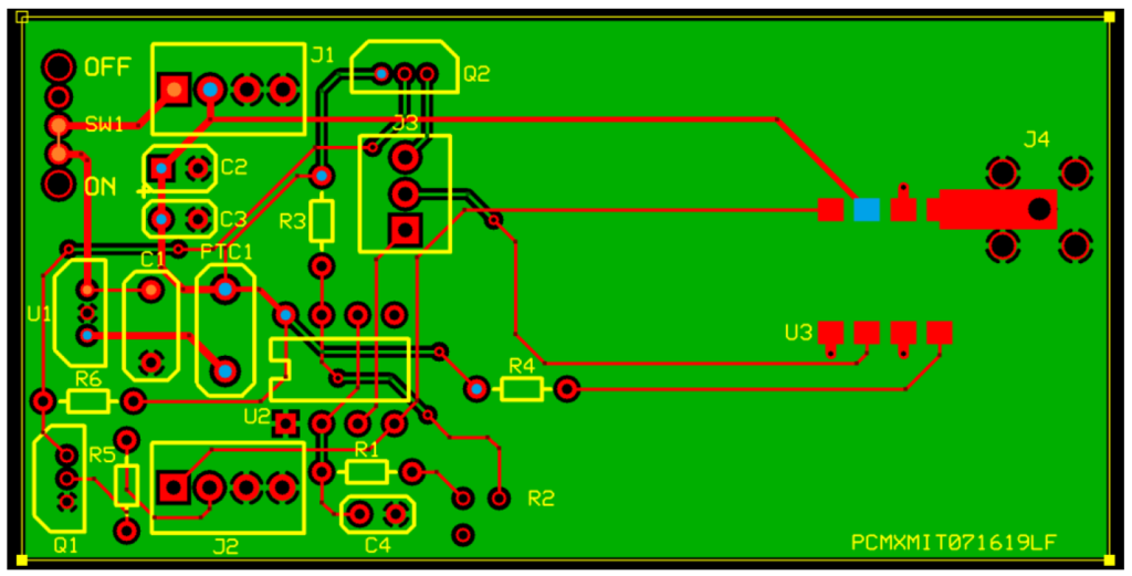
The Simple 315MHz Transmitter Module is contained on a 3.0″ x 1.5,” x 0.062″ two-sided, FR-4 epoxy glass printed circuit board with 1/2-ounce copper laminate. The lower side of the board contains the common ground plane, which serves as a 0.0VDC reference. Note, as seen in Figure 3, the transmitter and antenna connector are located close to the RH edge of the PCB, while the other components are located closer to the LH side. This layout assures minimal disturbance of the ground plane, allowing it to function effectively as a counterpoise for the antenna.

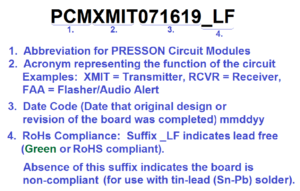
Figure 4 uses colors to represent the three layers of the Simple 315MHz Transmitter Module printed circuit board (PCB). Here, the ground plane and traces on the lower layer of the circuit board are represented in green, while traces and pads on the upper layer of the board are shown in red. Locations of components on the upper (silk-screen) layer of the PCB are shown in yellow. The lower RH corner of the module contains the PRESSON part number for the bare (unpopulated) PCB. (The PRESSON PCB part numbering system is explained in Appendix 3.) Table 1 lists and defines several of the reference designators used to identify components contained on PRESSON circuit boards.
| Table 1 – Common Component Designators | |
|---|---|
| Designation | Description |
| J (J1, J2, J3…) | Input/Output Connector |
| TP (Tp1, TP2, TP3…) | Test Point |
| JP (JP1, JP2, JP3…) | Jumper Position |
| R (R1, R2, R3…) | Resistor |
| C (C1, C2, C3…) | Capacitor |
| L (L1, L2, L3…) | Inductor |
| U (U1, U2, U3…) | Integrated Circuit (IC) |
| Q (Q1, Q2, Q3…) | Transistor |
| LED (LED1, LED2…) | Light Emitting Diode |
| PTC (PTC1, PTC2…) | Resettable Fuse |
| RT (RT1, RT2, RT3) | Thermistor |
| K (K1, K2, K3…) | PCB Relay |
| SW (SW1, SW2…) | Switch |
Simple 315MHz Transmitter Module Pin-In and Pin-Out: #
Figure 5 shows the pin-in/pin-out of the Simple 315MHz Transmitter Module. Four-position pin strip headers J1 and J2 are soldered to the ground plane side of the transmitter module PCB, allowing horizontal mounting of the module into a section of breadboard, or permanent connection to a user’s PCB.

+VBB, taken at pin 1 of connector J1, is the external DC supply voltage input. This voltage, which could be a standard value such as +5.0VDC, +9.0VDC, or +12.0VDC, serves as the input to a +3.3VDC point-of-load (POL) regulator onboard the transmitter module. (See U1 in Figure 3b and Figure 4.) While the POL regulator provides power to the transmitter IC and the square wave oscillator circuitry, it also provides a +3.3VDC output at pin 2 of J1. This +3.3VDC output could become the power source for ancillary devices such as the Linx LICAL-ENC-MS001 encoder. Pins 3 and 4 of J1 provide ground connection, to either the ground bus of a breadboard or the ground plane of a larger PCB.
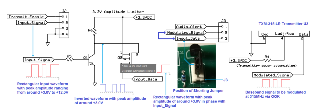
Transmit_Enable, taken at pin 1 of J2, is an active-high control signal that allows operation of the square wave oscillator (U2) and the 315MHz transmitter (U3). (See Figure 3b and Figure 4.) Holding this pin at a logic low (near ground potential) disables operation of both U2 and U3. Designated as Input_Signal, pin 2 of J2 accepts a pulsating DC rectangular wave form which can become the baseband signal modulated by the 315MHz transmitter. A level-shifting transistor switch at this input allows the peak amplitude of the baseband signal to range from around +3.0V to +12.0V. Per the datasheet for the TXM-315-LR transmitter, the data rate (or frequency) of the rectangular input waveform can approach 10,000 bits per second, equivalent to a 10Khz square wave. (The number of bits occurring within a second is commonly referred to as the BAUD rate) Pins 3 and 4 of J2 allow connection to system ground.
The Simple 315MHz Transmitter Module is designed to operate with a quarter wave 315MHz whip antenna having a reverse-polarity (RP) subminiature version A (SMA) connector. This small coaxial connector and whip antenna connect at the right-hand end of the transmitter module, as seen in Figure 5. The Linx ANT-315-CW-HWR-RPS antenna, included with the Simple 315MHz Transmitter/Receiver Pair, is designed to be swiveled into an upright position while the transmitter module is mounted horizontally on a breadboard or PCB.
Simple 315MHz Transmitter Module Power Distribution: #
Figure 6 shows a section of the Simple 315MHz Transmitter Module schematic diagram containing the components involved in +3.3VDC distribution. Figure 7 indicates +VBB and +3.3VDC termination points on the transmitter module. Pad locations for +VBB are indicated in orange, while +3.3VDC terminal points are indicated in blue.
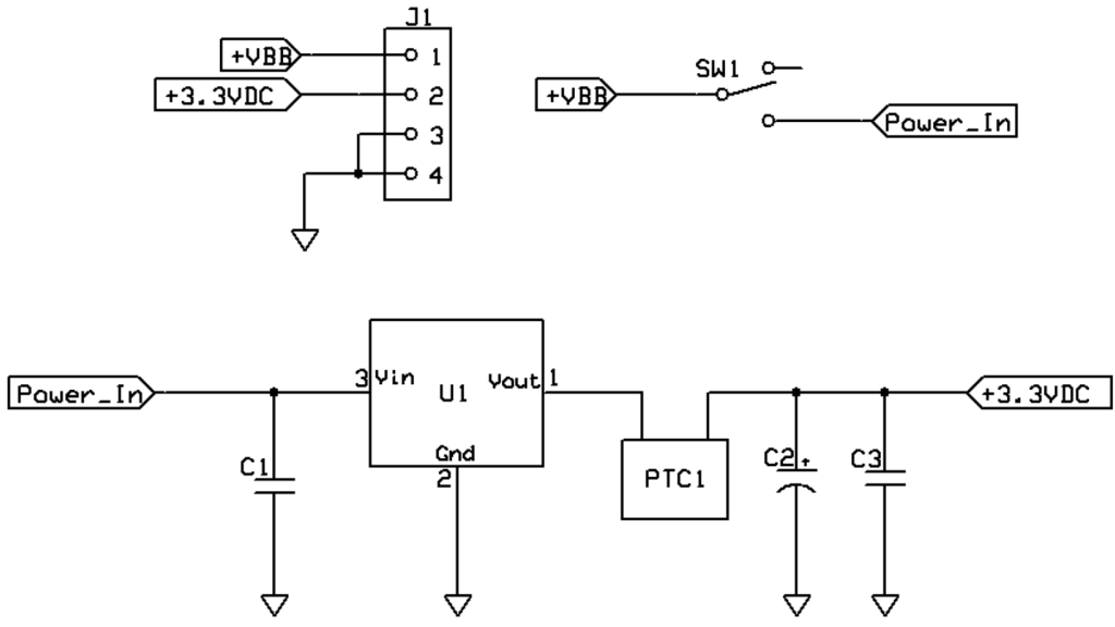
As seen in Figures 6 and 7, +VBB arrives at pin 1 of J1 and is present at the center pole position of single pole double throw (SPDT) slide switch SW1. Actuating the slide switch downward, as shown in Figure 7, applies +VBB to pin 3 of POL voltage regulator U1, which is a +3.3VDC load dropout (LDO) voltage regulator (STMicroelectronics part number L4931CZ33-AP). A key operating parameter of the LDO regulator operation is its dropout voltage (Vd). The dropout voltage is the difference between the rated output voltage of the regulator and the minimum level of input voltage that allows the device to maintain line and load regulation. Per the datasheet of the L4931CZ33-AP, Vd for the device could vary between 0.4 and 0.6V. Thus, for the Simple 315MHz Transmitter, +VBB input could decrease to between +3.7VDC and +3.9VDC and the L4931CZ33-AP could hold at +3.3VDC and still provide substantial output current. This is an ideal assumption, not taking into consideration the increased internal resistance of a battery in a low charge condition. The internal resistance of a battery is effectively in series with its load. Thus, as battery voltage decreases while the battery loses its charge, its current sourcing capability also decreases. Capacitor C1, a 0.47μF multilayer ceramic capacitor (MLCC), connects between pin 3 of voltage regulator U1 and circuit ground. C1 stabilizes the +VBB input and attenuates voltage spikes that could occur during commutation of slide switch SW1. The capacitor also shunts high frequency line noise toward circuit ground.
PTC1, connected directly to the +3.3VDC output of U1, is a resettable fuse (sometimes referred to as a polyswitch). For this device, PTC stands for its abrupt positive temperature coefficient. Assuming current through PTC1 remains at or below its 50mA holding value, the device behaves as a conventional fuse, offering nearly zero ohms of resistance. If series current increases toward a trip value of 100mA, possibly due to a partial short circuit, the resultant self-heating of PTC1 causes its resistance to abruptly increase. With PTC1 acting as a high resistance in series with the +3.3VDC source, circuit current is attenuated. To restore the module to normal operation, the +VBB power source must be momentarily removed, and the short circuit condition must be remedied. Once this occurs, PTC1 will again exhibit nearly zero ohms of series resistance.
Capacitors C2 and C3 provide stabilization and filtering for the +3.3VDC bus. C2 is a 10μF, 6.3V tantalum capacitor. While tantalum capacitors provide high values of capacitance in small packages sizes, they also exhibit relatively high values of equivalent series resistance (ESR). To compensate for the high ESR of capacitor C2, capacitor C3, a 0.01μF, 50V MLCC, is placed in parallel with that component.
Because a ceramic capacitor has a very low ESR, the parallel ESR of C2 and C3 is less than the ESR of C3.
As has been explained, pin 2 of J1 can provide +3.3VDC to an external low power load such as an encoder IC. However, the user should ensure the combined current drawn from an external load and the transmitter module (while active) does not exceed the 50mA holding current of PTC1. As shown in Figure 7 and the complete schematic diagram for the Simple 315MHz Transmitter Module (Appendix 2), +3.3VDC becomes the operating voltage for the square wave oscillator circuitry containing U2 and transmitter IC U3. It also becomes the biasing voltage for the level-shifting transistors Q1 and Q2.
Simple 315MHz Transmitter Input Signal Channel: #
As shown in Figure 8, the signal to be modulated by the Simple 315MHz Transmitter Module is taken at pin 2 of header J2. A transistor switching stage, containing npn transistor Q1 and p-channel MOSFET Q2, allows the peak amplitude of the rectangular Input_Signal waveform to range from around + 3.0V to +12.0V. During the high state of the Input_Data signal, Q1 is switched on in saturation, pushing the gate voltage of Q2 to near ground potential. With this action, Q2 is switched on, pulling the Input_Data signal to a peak level of nearly +3.0VDC, a safe high input level for the TXM-315-LR transmitter IC (U3). A logic low at pin 2 of J2 places Q1 in a cut-off condition, pulling its collector voltage toward +3.3VDC. This action turns off Q2, holding the Input_Data signal near ground potential. This inversion of the inverted input signal keeps the Input_Data signal at the drain terminal of Q2 in phase with the Input_signal arriving at pin 2 of J2.
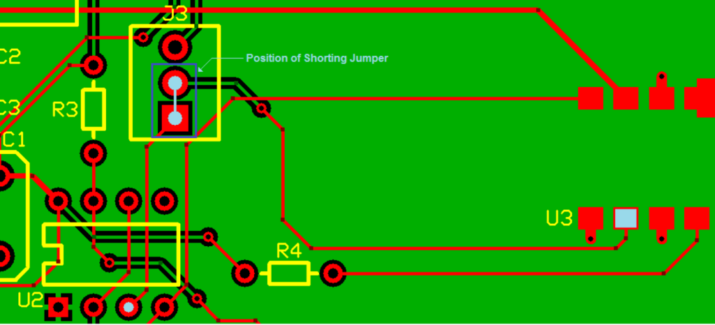
Three-position pin strip header J3 allows selection of the input signal source for the data input to the TXM-315-LR transmitter IC. Placing a shorting jumper (or shunt) over pins 2 and 3 of J3, as illustrated in Figure 8, allows the Input_Data signal to become the Modulated_Signal that arrives at pin 2 of U3. As seen in Figure 2, this signal is modulated by the 315MHz carrier using on-off keying (OOK). Placing the shunt between pins 1 and 2 of J3 allows continuous modulation of the 4.0KHz Audio_Alert signal while the transmitter is enabled.
Simple 315MHz Transmitter Module 4.0KHz Square Wave Oscillator: #
Figure 9 contains the circuitry for the Simple 315MHz Transmitter Module Square Wave Oscillator. U2 is a Renesas/Intersil ICM7555IPAZ general purpose CMOS timer, configured to operate as an astable multivibrator (free running rectangular waveform generator). The active high Transmit_Enable input from pin 1 of J2 is routed to pin 4 of U2, the timer’s active-low reset input. This logic high at pin 4 of the timer allows continuous operation of the square wave oscillator circuitry. A logic low at this input inhibits operation of U2, holding the timer’s Audio_Alert output at a logic low. This reset state of the timer is concurrent with the power-down condition of the TXM-315-LR transmitter IC (U3).
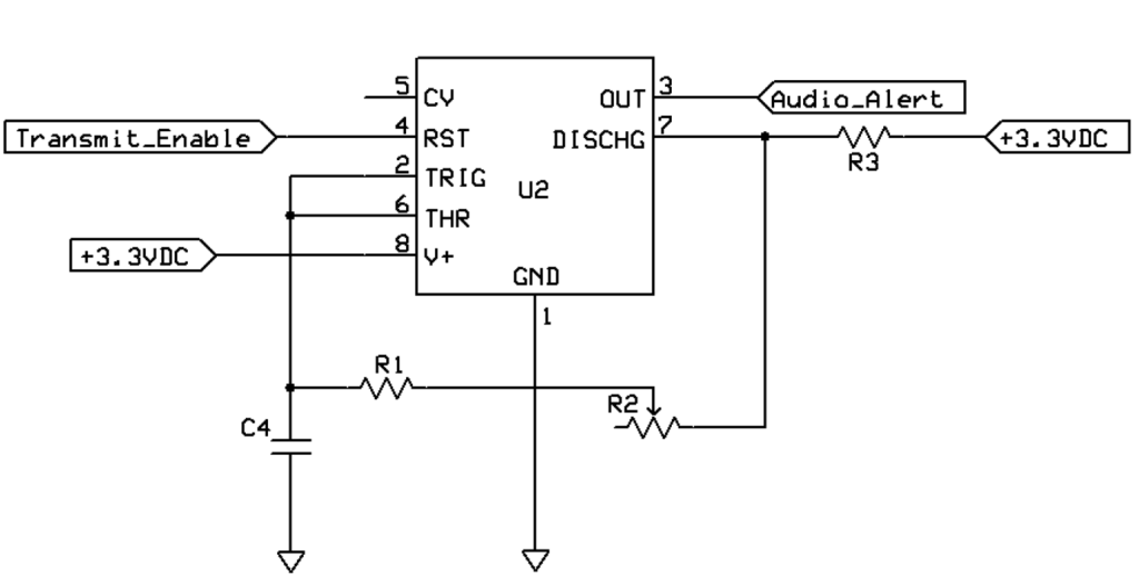
For the square wave oscillator in Figure 9, pulse width (PW) is the time in which its Audio_Alert output signal at pin 3 of U2 is in a logic high state. Pin 3 holds at a logic high (nearly +3.0VDC) while capacitor C4 charges via resistors R1, R2, and R3. During this charging cycle, these three resistors are effectively in series. When capacitor C4 attains a voltage level of nearly 2/3 the supply voltage (+2.2VDC), the voltage at pin 3 falls low. During the space width (SW) of the Audio_Alert signal, C4 discharges via R1 and R2 into pin 7 of U2. At the instant the voltage over C4 decreases to 1/3 the level of the supply voltage (+1.1VDC), the output at pin 3 returns to nearly +3.0VDC and C4 begins to charge again via R1, R2, and R3. The duration of the pulse width is determined as shown by Equation 1. Here, 20KΩ trimmer resistor R2 is assumed to be set to its midpoint ohmic value of 10KΩ. As indicated in Appendix 1, capacitor C4 equals 0.01μF, R1 equals 6.8KΩ, and R3 equals 1KΩ. For the following calculations, assume the square wave oscillator has been running for several cycles and the lower threshold of capacitor voltage has stabilized at approximately 1/3 of the supply voltage (+1.1VDC).
Equation 1
During the space width of the Audio_Alert signal, the discharge path for capacitor C4 is through just R1 and R2. Thus, space width is slightly shorter than the pulse width, determined as shown in Equation 2.
Equation 2
The period of the Audio_Alert signal (T) is equivalent to PW + SW, while the frequency of that signal is the reciprocal of the period. As shown in Equation 3:
Equation 3
The Audio_Alert output of the square wave oscillator can serve as a beacon signal for verifying the range of the Simple 315MHz Transmitter/Receiver Pair. R2 is a small 20KΩ, single turn trimmer resistor that allows fine adjustment of the Audio_Alert signal frequency. As demonstrated by the above three equations, pre-adjusting the trimmer to its midpoint value of around 10KΩ should bring the Audio_Alert frequency very close to 4.0KHz, which is the specified resonant frequency of the piezoelectric audio transducer on the Simple 315MHz Receiver module. With the receiver module configured to demodulate the 4.0KHz beacon signal, a one-time final adjustment of trimmer R2 should be made to allow for the strongest and clearest tone from the receiver’s piezo transducer. The user could then determine the distance from the transmitter module at which the demodulated piezo signal begins to deteriorate. For example, if the transmitter and receiver modules are 110 feet apart at the point where the 4.0KHz tone begins to break up, then the user could assume reliable simplex (unidirectional) data communication could occur up to about 100 feet. There are other factors to consider in determining the working range of transmission, including the amount of interference in the area, as well as the BAUD rate for an asynchronous communication system. During experimental procedures contained in the PRESSON courseware, squelch control circuitry will be implemented at the receiver side of the communication link to inhibit noise, but with a tradeoff of reduced transmission range.
As explained earlier, three-position pin strip header J3 allows selection of the source of the input signal for the TXM-315_LR transmitter IC. Placing the shorting jumper (or shunt) over pins 1 and 2 of J3, as illustrated in Figure 10, allows the 4.0kHz Audio_Alert signal, originating at pin 3 of general-purpose timer U2, to become the Modulated_Signal arriving at pin 2 of the TXM-315-LR transmitter.
TXM-315-LR Transmitter and Antenna Feed: #
The LR Series Transmitter Module Data Guide is a valuable source of information about the TXM-315-LR transmitter contained on the Simple 315MHz Transmitter Module. As shown on page 8 of that document, the 315MHz carrier for this device is generated by a voltage-controlled oscillator (VCO) contained within a phase-locked loop (PLL). While a detailed analysis of VCO and PLL technology is beyond the scope of this document, a brief explanation of a PLL could help in understanding the operation of the TXM-315_LR transmitter. While the illustration on page 8 of the data guide is essentially correct, the transmitter PLL forms a complete feedback loop containing the elements shown by the block diagram in Figure 11.

For a VCO, the DC control voltage determines the frequency of oscillation for the device. Typically, lowering the control voltage for the VCO increases its output frequency, while increasing the control voltage decreases frequency. The Phase Comparator stage of the PLL continually compares the phase relationship between the output of the VCO and a reference frequency. As shown in Figure 11, the reference frequency is produced by a crystal oscillator. In this example, we could assume the crystal resonates at 315MHz. If the VCO output frequency begins to lag behind or increase above the reference value, the phase comparator senses the resultant disparity in frequency and sends a corrective signal to the VCO via the low-pass filter stage. The output of the low-pass filter is the DC control signal, which changes in amplitude as necessary to bring the VCO output back to its reference value.
As shown in Figure 11 of this document, as well as Figure 8 of the LR Series Transmitter Module Data Guide, the VCO output becomes the input to a power amplifier. The power amplifier boosts the strength of the carrier signal to a level that allows it to radiate from the attached antenna. As shown in Figure 8 of the data guide, the modulated baseband signal, indicated as DATA, is in a logic AND relationship with the PDN (power-down) signal. The TXM-315-LR transmitter can only operate when the PDN is in a logic high state. This high condition at pin 8 of U3 enables operation of the PLL circuitry and allows the DATA signal to pass directly to the power amplifier stage. As explained earlier, with the OOK method of modulation, the carrier is totally absent during the space time of the DATA signal. As illustrated in Figure 12 below, assuming PDN is high, the Ant output of the transmitter consists of a burst of the 315MHz carrier occurring during each high state at the Modulated_Signal.
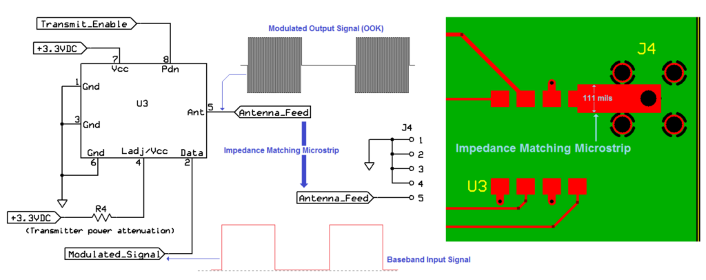
The PRESSON Simple 315MHz Transmitter Module design allows connection of a 315MHz whip antenna directly to RP-SMA coaxial connector J4. To achieve optimal performance of the transmitter and antenna, the designer must take care in fabricating the microstrip, a short section of trace material that effectively becomes a transmission line between the transmitter output and the antenna feed point. Valuable information about microstrip design is provided in the Microstrip Details, on page 19 of the data guide. Ideally, for optimal power transfer, the characteristic impedance of the microstrip should equal the input impedance of the antenna. For the Simple 315MHz Transmitter Module, a microstrip characteristic impedance of 50Ω is required to match antenna input impedance. This microstrip impedance is achieved with a trace width of 111 mils (0.111”). This trace width is specified with the assumption that the PCB is 0.062″ thick and fabricated with FR-4 epoxy glass. All PRESSON PCBs are, in fact, 0.062″ thick and fabricated with FR-4 epoxy glass. (See page 3 of this document.)
While the use of a stabilizing ground plane is always advisable for any multi-layer PCB design, it is essential for proper operation of the Simple 315MHz Transmitter Module. The board is designed to operate with a quarter wave, 315MHz antenna, such as the Linx ANT-315-CW-HWR-RPS shown in Figure 13, being attached to coaxial connector J4.

For reliable operation, the transmitter module and antenna must together develop one-half of the carrier waveform. This can be accomplished with a quarter wave antenna, providing there is enough ground plane area to function as a counterpoise, developing the additional quarter wave component of the radiated carrier. To ensure sufficient counterpoise function, the designer must keep the PCB ground plane as undisturbed as possible. This is particularly challenging for a PCB that has through-hole components. As seen with the Simple 315MHz Transmitter Module, through-hole components are moved toward the left-hand side of the PCB, with the transmitter and antenna connector moved toward the RH side. Traces on the ground plane layer, though sometimes necessary, are kept to a minimum and made as short as possible, extending lengthwise across the ground plane of the PCB.
The Simple 315MHz Receiver Module Structure and Layout: #
The Simple 315MHz Receiver Module is contained on a 2.85″ x 1.4″ x 0.062″ two-layer, FR-4 epoxy glass printed circuit board with half-ounce copper laminate. The lower layer of the board contains the ground plane. Note, as seen in Figure 14, the receiver and antenna connector are located close to the RH edge of the PCB, while the other components are located closer to the bottom edge and LH side of the module. This layout assures minimal disturbance of the ground plane, allowing it to function effectively as a counterpoise for the surface mount antenna.
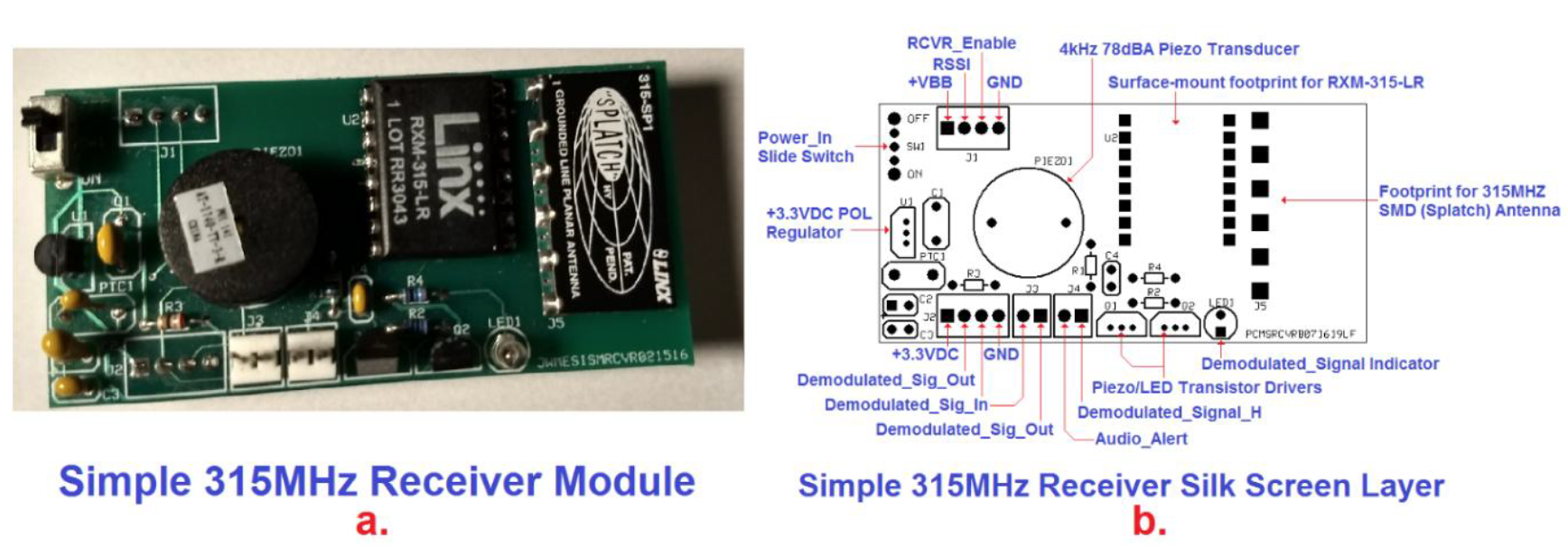
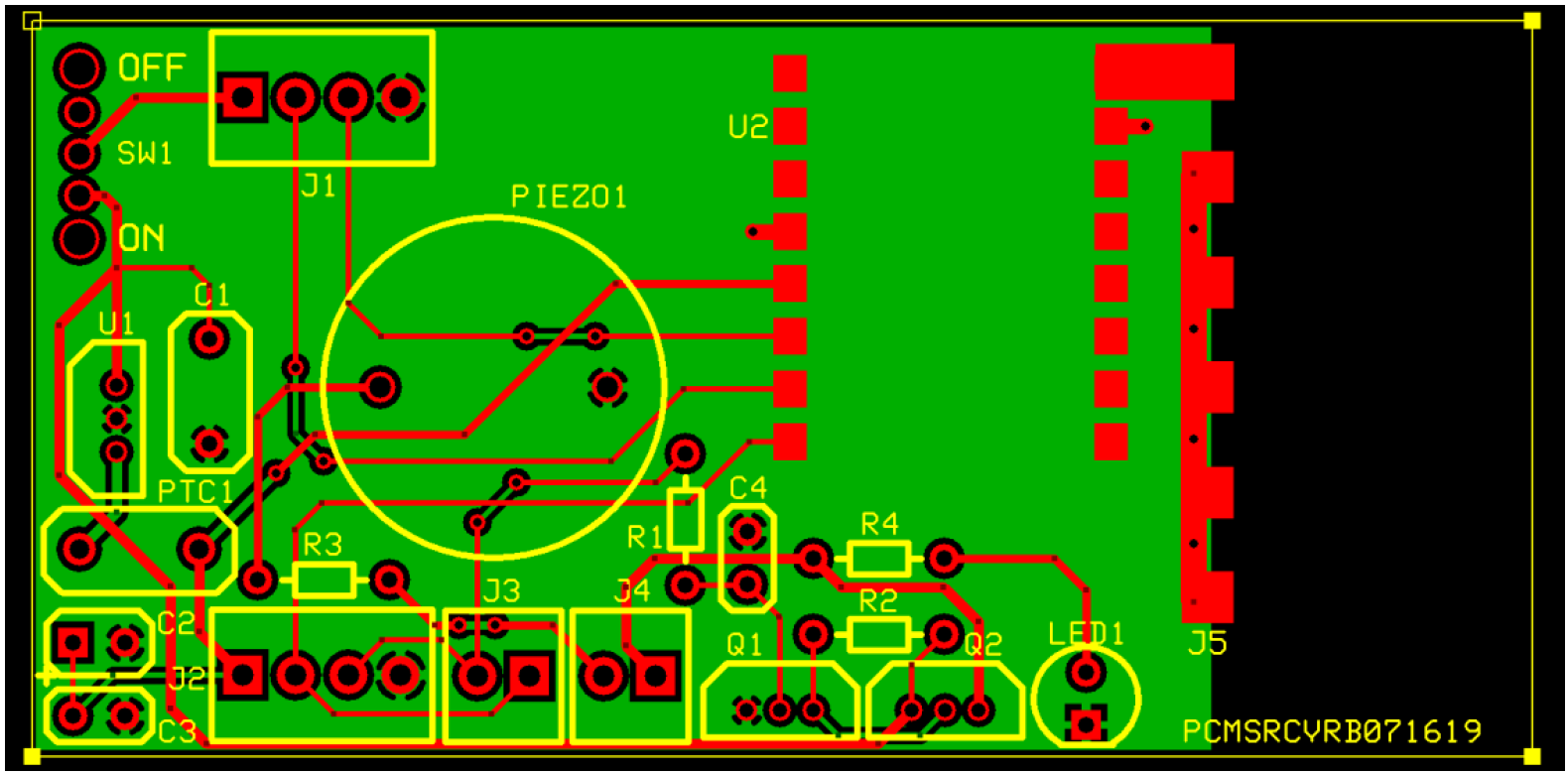
Figure 15 uses colors to represent the three layers of the Simple 315MHz Receiver Module printed circuit board (PCB). Here, the ground plane and traces on the lower layer of the circuit board are represented in green, while traces and pads on the upper layer of the board are shown in red. Locations of components on the upper (silk-screen) layer of the PCB are shown in yellow. The lower RH corner of the module contains the PRESSON part number for the bare (unpopulated) PCB. (The PRESSON pg. 19
PCB part numbering system is explained in Appendix 3.) Table 1, on page 4 of this document, lists and defines several of the reference designators used to identify components contained on PRESSON circuit boards.
Simple 315MHz Receiver Module Pin-In and Pin-Out: #
Figure 16 shows the pin-in/pin-out of the Simple 315MHz Receiver Module. Four-position pin strip headers J1 and J2 are soldered to the ground plane side of the transmitter module PCB, allowing horizontal insertion of the module into a section of breadboard, or direct connection into a user’s PCB.
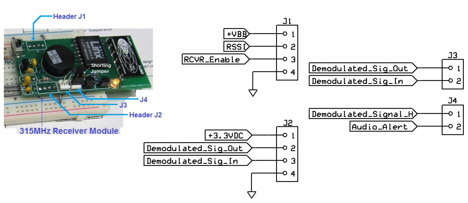
+VBB, located at pin 1 of connector J1, is the input for the external DC supply voltage. As with the transmitter module, this source voltage is present at the center pole position of SPDT slide switch SW1. Actuating the slide switch downward applies +VBB to pin 3 of +3.3VDC point-of-load (POL) voltage regulator U1 (part number L4931CZ33-AP). This regulator is identical to that contained on the Simple 315MHz Transmitter module. It accepts common +VBB input voltages such as +5.0VDC, +9.0VDC, or +12.0VDC. As seen in Figure 14b and Figure 15, POL regulator U1 serves as the power source for the RXM-315-LR IC and also provides a +3.3VDC output at pin 1 of J2. This +3.3VDC output could provide power to ancillary devices such as the Linx LICAL-DEC-MS001 decoder. (The pin 4 positions of both J1 and J2 provide a connection to either the ground bus of a breadboard or the ground plane of a larger PCB.
The Received Signal Strength Indicator (RSSI) output from the RXM-315-LR receiver is present at Pin 2 of J1. Taken at pin 7 of that device, the RSSI signal is a pulsating DC voltage, the amplitude of which varies in direct proportion to the strength of any detected radiant energy within the receiver’s passband (whether it be the desired modulated carrier or spurious RF noise). Pages 10 of the RXM-315-LR Data Guide provides a detailed explanation of the RSSI function and identifies a few of its possible applications. Page 11 of that document contains a reference design for a squelch control circuit utilizing the RSSI feature of the RXM-315-LR receiver. A lesson within Course PCMT6C2 (part of Track Six of the PCM eLearning Courseware) provides an opportunity for students to breadboard and test a squelch control circuit similar to that shown on page 11 of the RXM-315-LR Data Guide. (The breadboarded circuitry could appear as shown in Figure 20 of this document.)
The Receiver_Enable input, taken at pin 3 of J1, is an active-high control input that allows operation of the RXM-315-LR receiver (U2). This input connects directly to the PDN (Power Down) input of the receiver (pin 6 of U2). The Receiver_Enable input allows full operation of the RXM-315-LR IC when at a logic high and puts the receiver into a low power (sleep) state when at a logic low.
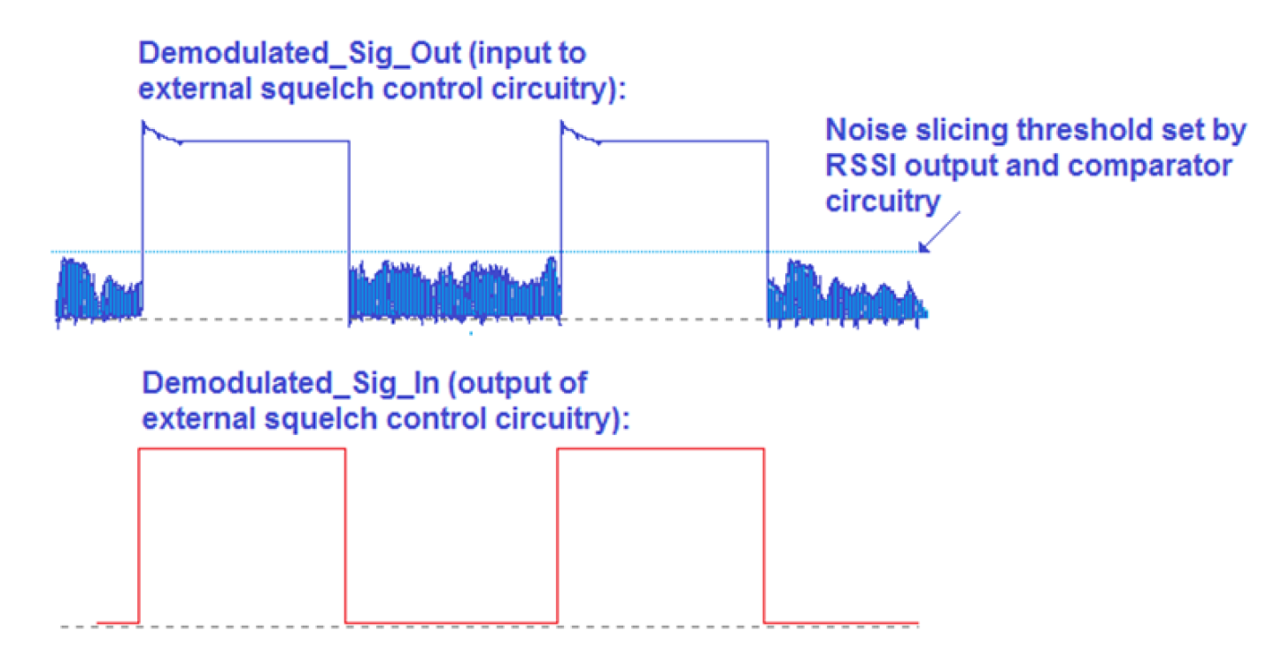
The Demodulated_Sig_Out signal, taken at pin 2 of J2, is common to the Data terminal of U2. While the user could recover the modulated baseband signal data directly at pin 8 of the RXM-315-LR receiver, it is often necessary to further condition the received signal, possibly feeding it through squelch control circuitry, which could block the lower-amplitude white noise component of the received signal. As indicated in Figure 17, the data output of the squelch control circuit, with noise removed, could become the Demodulated_Sig_In signal at pin 3 of J2.
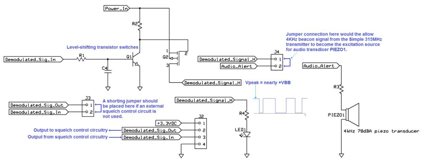
As shown in Figure 18, the Demodulated_Sig_In signal becomes the base input to the inverting transistor switch Q1. Here, R1 and C4 form a first order low-pass filter, attenuating high-frequency noise that could be present at pin 3 of J2. A peak amplitude as low as +3.0V at Demodulated_Sig_In is sufficient to drive Q1 into saturation, pushing its collector output toward 0.2V. This near ground level at the gate of p-channel MOSFET Q2 causes that transistor to conduct, pulling its drain voltage, Demodulated_Signal_H, toward +VBB. This high voltage condition causes LED1 to illuminate. The value of R4 (510Ω) allows LED current to approach its rated value of nearly 20mA with +VBB at its maximum recommended value of +12.0VDC. As indicated in Figure 18, assuming the transmitter module is sending its 4.0KHz beacon signal to the receiver module, placing a shorting jumper, or shunt, over two-position header J4 allows that signal to become the excitation source for audio transducer PIEZO1. If the user’s application does not require external squelch circuitry, but does need access to LED1 and PIEZO1, shorting jumpers should be placed across both J3 and J4. By not conditioning the recovered 4.0KHz beacon signal via an external squelch control circuit, the user could extend the operating range between transmitter and receiver. However, a trade off could be constant static noise emanating from Piezo1 while the beacon signal is not present.
RXM-315-LR Receiver and Antenna Feed: #
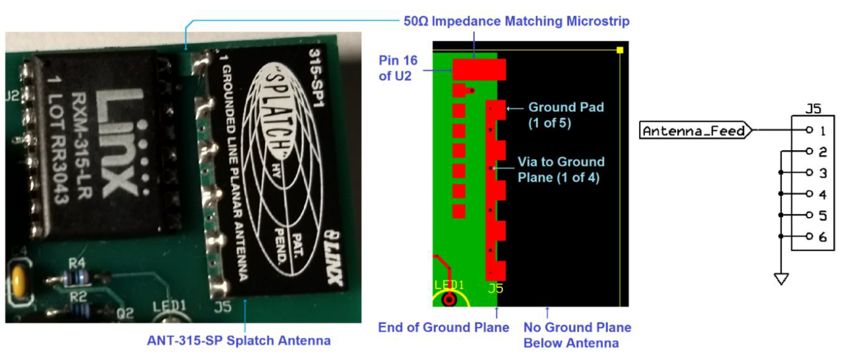
The Simple 315MHz Receiver Module contains a Linx Splatch antenna, tuned to the 315MHz carrier radiated by the whip antenna attached to the Simple 315MHz Transmitter Module. The term Splatch™ appears to be a clever combination of the terms splotch (a spot or mark), patch, and planar. The terms patch and planar are commonly used to describe a small, low-profile antenna that mounts directly on the surface of a PCB. As shown in Figure 19, the captured 315MHz carrier signal is sent to the Antenna_Feed input (pin 16) of receiver U2 via a 50Ω impedance matching microstrip. The design of the PCB antenna footprint and mounting location of the Simple 315MHz Receiver Module adheres to the recommendations contained in the datasheet for the ANT-315-SP antenna. As illustrated in Figure 19, to ensure optimal counterpoise function of the ground plane, the Splatch antenna is mounted at the RH side of the receiver module, directly over the edge of the lower ground plane layer. Pad 1 of the ANT-315-SP is the Antenna_Feed terminal, which connects to the Ant input of U2 (pin 16) via the microstrip. Pads 2 through 6 are connected by a single, 0.05” wide trace on the upper layer of the PCB. As shown in Figure 19, four vias connect this common trace to the ground plane on the lower layer of the PCB.
The RXM-315-LR receiver module contains a superheterodyne receiver, shown in block form in Figure 11 on page 8 of the RXM-315-LR Data Guide. Superheterodyne receiver operation is covered in detail in Course PCMT6C1 (part of Track Six of the PCM eLearning Courseware). While a detailed explanation of that process is beyond the scope of this document, a general description of the receiver operation is given on page 9 of the RXM-315-LR Data Guide.
Tuned to a center frequency (the 315MHz carrier), the ANT-315-SP antenna is sensitive to desired signals (intelligence), as well as RF noise within its 5.0MHz passband. Ideally, 315MHz would be at the exact center of the antenna passband. However, the data guide for the ANT-315-SP specifies a frequency range of 312MHz to 317MHz. As represented in Figure 11 on page 8 of the RXM-315-LR Data Guide, the Antenna_Feed connects to a band select (bandpass) filter. The purpose of this initial stage of the receiver is to reject RF noise present within the antenna passband. The band select filter passes the modulated 315MHz carrier to a cascode low-noise amplifier (LNA) stage. (A cascode amplifier is a form of transconductance amplifier featuring high gain and excellent noise rejection.)
The receiver’s heterodyning action occurs within the double-balanced mixer stage. Here, the output of the LNA, the filtered and amplified 315MHz carrier signal, is intermodulated with the output of the local oscillator. The local oscillator stage consists of a phase-locked loop (PLL), similar to that shown in Figure 11 of this document. One of the products of the mixing process is a difference frequency (fcarrier – fPLL). (Because the specified difference, or intermediate frequency is 10.7MHz, we could assume the crystal-synchronized PLL frequency to be 304.3MHz.) The subsequent intermediate frequency (IF) stage further amplifies the 10.7MHz signal which now contains the modulated baseband signal.
Demodulation of the baseband signal occurs with further low-pass filtering and amplification of the IF signal. The output of the limiter stage becomes the input to a voltage follower amplifier, the output of which becomes the RSSI output at pin 7 of U2. Before becoming the Data output at pin 8 of U2, the recovered baseband signal must undergo the necessary wave shaping. The final, data slicing, stage in the block diagram on page 8 of the data guide appears to contain a Schmitt triggered buffer amplifier. The purpose of this stage of the circuitry is to sharpen the leading and lagging edges of the recovered signal, making it more rectangular. The process of data slicing can also involve a squelching action, establishing a noise threshold as shown in Figure 17 of this document. As explained earlier, external squelch circuitry can also perform data slicing, integrating the RSSI output and comparing it to a switching threshold voltage.
Simple 315MHz Transmitter and Receiver Module Pair Applications: #
Course PCMT6C2 (part of Track Six of the PCM eLearning Courseware) contains two introductory exercises involving just the Simple 315MHz Transmitter and Receiver Module Pair. The first exercise involves a simple range check. The second exercise involves fabrication and testing of squelch control circuitry for the receiver module, followed by a repetition of the range check. As shown in Figure 20, the Simple 315MHz Transmitter and Receiver Module Pair can be used in a variety of applications involving other PRESSON Circuit Modules.
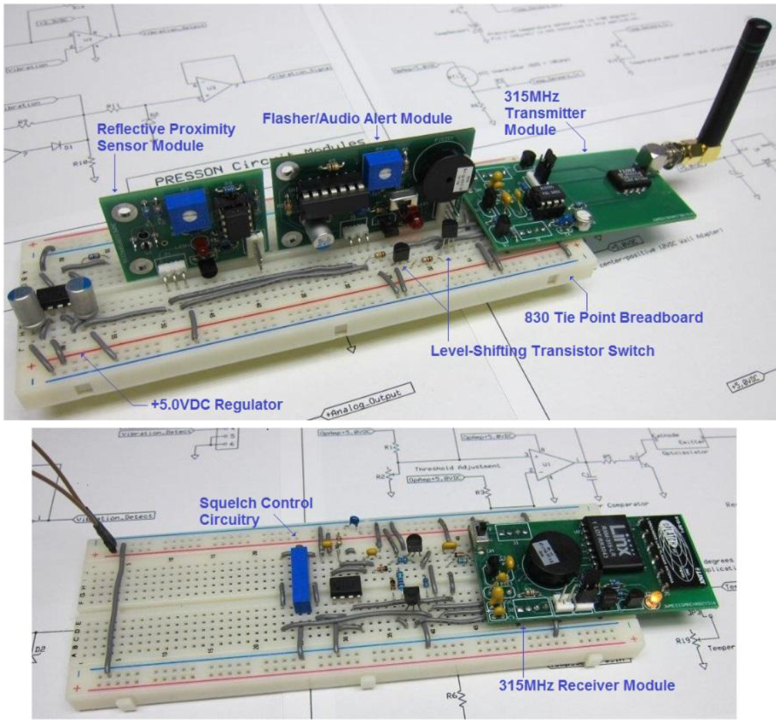
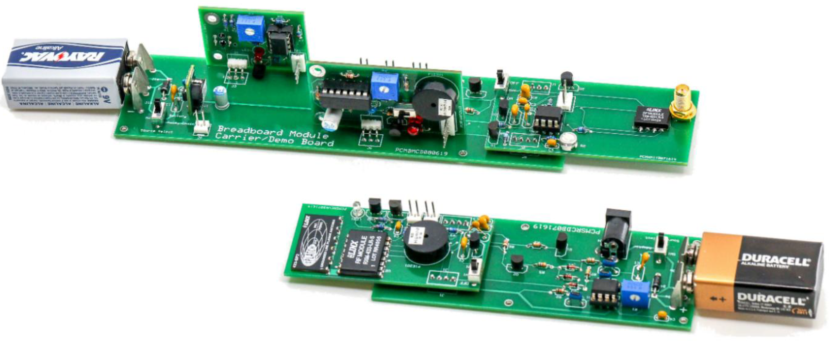
Figure 21 contains special order carrier boards that allow permanent connection of the circuitry shown in Figure 20. The carrier board containing the transmitter module is quite versatile, allowing for a variety of applications, ranging from remote sensing to wireless transfer of data from one MCU to another. For further information, please refer to user’s manuals for the PRESSON Breadboard Module Carrier/Demo Board, Squelch Receiver Carrier/Demo Board, and Sensor Sampler Carrier/Demo Board.
Appendix 1: #
The following is a complete listing of components comprising the Simple 315MHz Transmitter Module and Simple 315MHz Receiver Module. With the exception of the PCMXMIT071619 and PCMSRCVRB071619 PCBs, replacement parts for the module can be ordered from Mouser Electronics. The blank PCB can be ordered from PRESSON Circuit Modules, Inc. NOTE: The two PCBs specified above are designed for assembly using legacy tin/lead Tin-lead (Sn-Pb) solder. RoHS compliant (lead free) versions of the two PCBs can be ordered as PCMXMIT071619_LF and PCMSRCVRB071619_LF.
Bill of Materials: Simple 315MHz Transmitter Module
| Table 2 – Bill of Materials | ||
|---|---|---|
| Component | Description | Product Number |
| C1 | 0.47uF 50V Z5U MLCC | 80-C322C474M5U |
| C2 | 10uF 6.3V 10% tantalum | 594-K103K15X7RF53L2 |
| C3 | 0.01uF, 50V MLCC | 80-C320C103M5R |
| C4 | 0.01uF 50V C0G 5% MLCC | 810-FK18C0G1H103J |
| J1 | 4p 0.1″ pin strip header | 571-6404524 |
| J2 | 4p 0.1″ pin strip header | 571-6404524 |
| J3 | 3p 0.1″ pin strip header | 571-6404523 |
| J4 | RPSMA 50ohm R A jack | 712-CONREVSMA002-L |
| PTC1 | 50mA hold/100mA trip polyswitch | 650-RXEF005 |
| Q1 | MPSA20 npn small signal | G19467 |
| Q2 | 40V P-channel enhancement RDS(on) = 8ohm | 689-VP0104N3-G |
| R1 | 6.8Kohm 1/8W 1% metal film | 270-6.8K-RC |
| R2 | 20Kohm 1/2W 10% single-turn trimmer | 652-3329H-1-203LF |
| R3 | 1Kohm 1/8W 1% metal film | 270-1K-RC |
| R4 | 2.7Kohm 1/8W 1% metal film | 270-2.7K-RC |
| R5 | 29.4Kohm 1/8W 1% metal film | 270-29.4K-RC |
| R6 | 1Kohm 1/8W 1% metal film | 270-1K-RC |
| SW1 | SPDT slide switch | 611-S102011MS2QN1 |
| U1 | 3.3V 100mA Positive Regulator | 511-L4931CZ33-AP |
| U2 | 315MHz receiver module | 712-RXM-315-LR |
| RCVR_PCB | 2.85″ x 1.4,” x 0.062″ two-layer, FR-4 | PCMSRCVRB071619 |
Appendix 2: #
Figure 22 contains the complete schematic diagram of the circuitry comprising the PRESSON Simple 315MHz Transmitter Module.
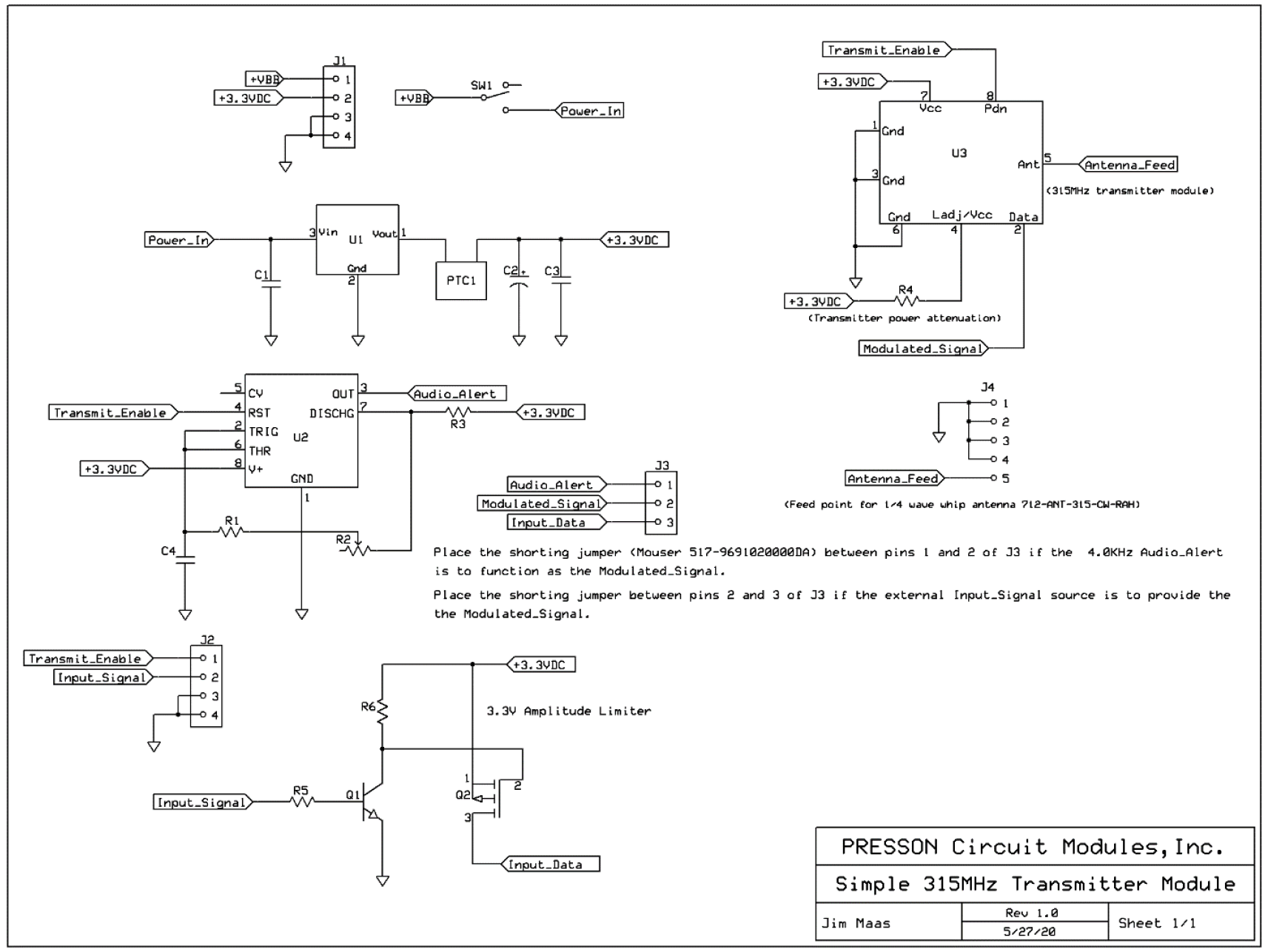
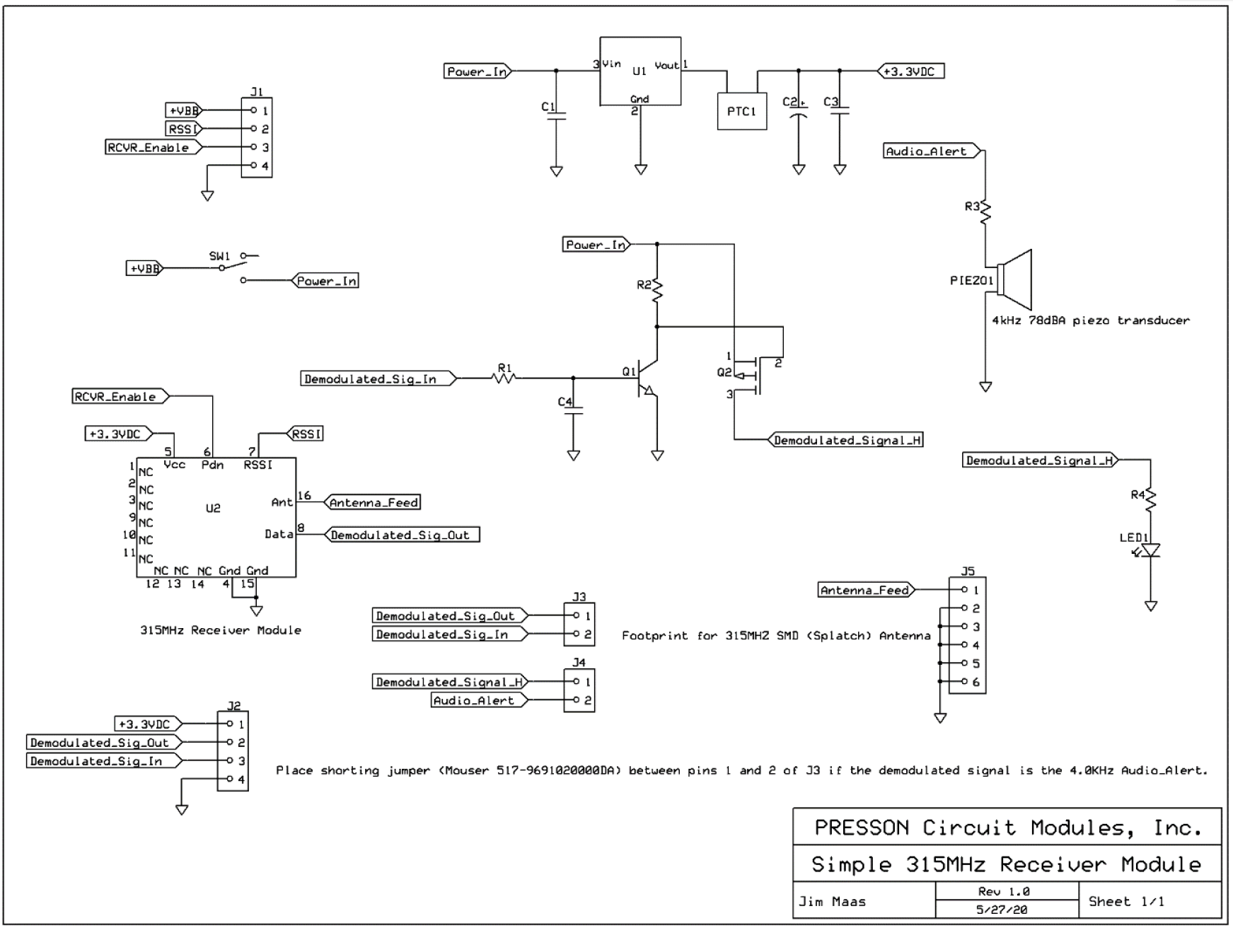
Figure 23 contains the complete schematic diagram of the circuitry comprising the PRESSON Simple 315MHz Receiver Module.
Appendix 3 #
Anatomy of a PRESSON PCB Stock Number
