Downloads #
Introduction #
The PRESSON C51 Microcontroller Project Launcher is a free-standing circuit module designed to serve as a platform for experimentation and project development using the Silicon Labs C8051F330-GM MCU (microprocessor control unit). In the datasheet for the C8051F330-GM MCU, the manufacturer describes the device as a “system on a chip MCU.” This description is appropriate because of the rich assortment of peripherals within the IC (integrated circuit) package, operating in support of the embedded 8051 CPU (central processing unit). These peripherals include numerous programmable timers and counters, a 10-bit ADC (analog-to-digital converter), a current-sourcing DAC (digital to analog converter), a UART (universal asynchronous receiver/transmitter), an enhanced serial peripheral interface (SPI), and a system management bus (SMB) interface.
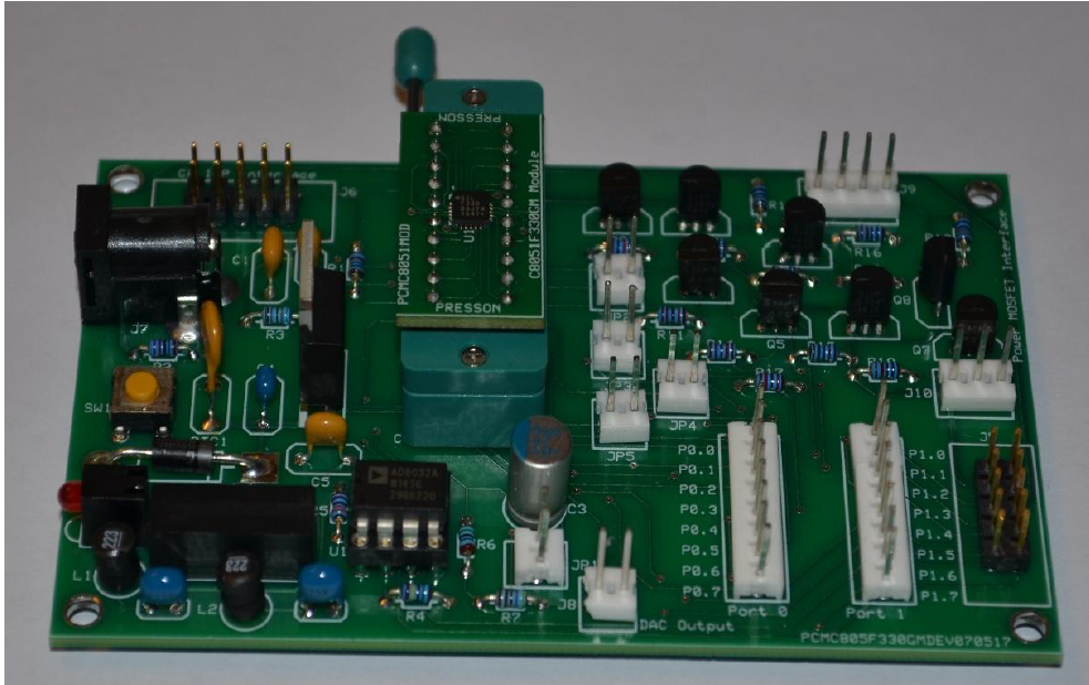
PRESSON Circuit Modules, Inc. provides a comprehensive set of lab/theory exercises covering real world applications of the peripherals contained within the C8051F330-GM MCU. A feature of the C51 Microcontroller Project Launcher Circuit Module that makes it particularly desirable for experimentation and project development is the removable C8051330GM DIP-20 MCU Module. During programming and experimentation, the module fits securely into either a standard DIP-20 IC socket or an optional DIP-20 ZIF socket located near the center of the project launcher module. When initial programming and experimentation is completed, the user can quickly remove the module and placed it into any standard breadboard or protoboard with a 0.1″ grid. If a project requires further programming revisions or debugging, the user can easily remove the module from the project board and re-insert it into the IC socket on the project launcher. (See ordering options for this product at the PRESSON website.)
Printed Circuit Board Specifications #
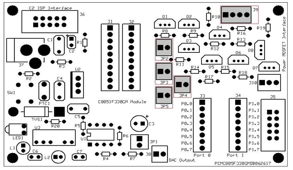
The PRESSON C51 Microcontroller Project Launcher is contained on a two-layer FR-4 epoxy glass PCB (printed circuit board) with 1/2 oz copper laminate. The board dimensions are 4.0″ x 2.5.” The lower layer of the board contains a ground plane, with grounded 0.125″ mounting holes in the four corners. These holes allow for panel mounting of the PCB, with possible chassis grounding to a metal enclosure or base plate. The user is strongly encouraged to purchase the Ancillary Kit for the C51 Microcontroller Project Circuit Module. This kit contains PCB standoffs that elevate the module and protect its bottom layer from damage. Figure 1 shows the silk-screening on the upper layer of the PCB, clearly indicating the location of each component.
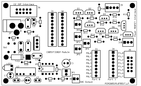
Figure 2 uses colors to represent the two layers of the C51 Microcontroller Project Launcher. Here, the ground plane and traces on the lower layer of the circuit board are represented in green, while traces, pads, and vias on the upper layer of the board are shown in red. The locations of components on the upper, silk screen layer of the PCB are shown in yellow.
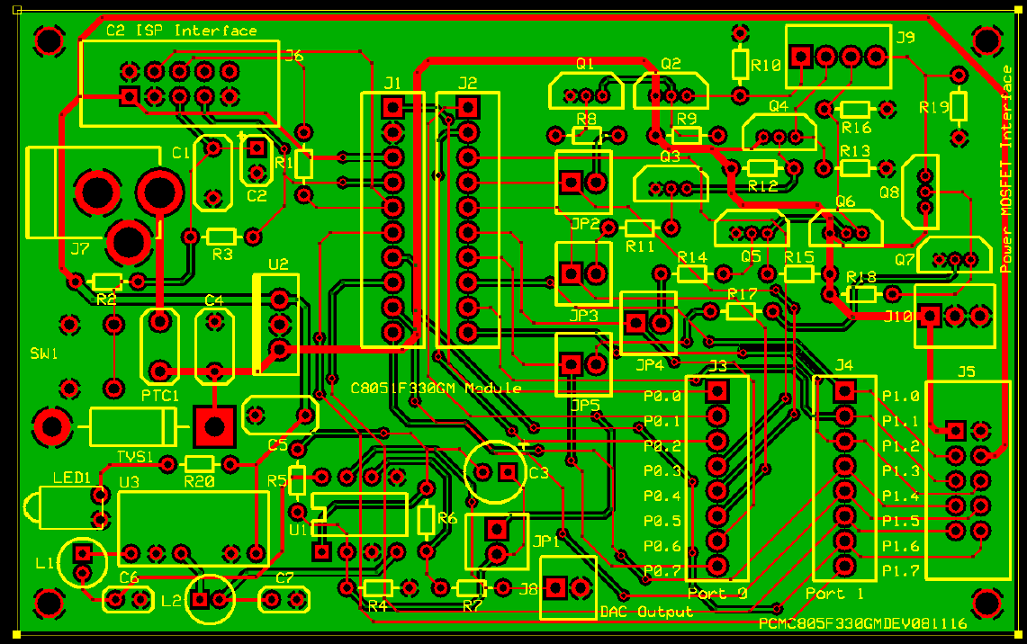
Table 1 lists and defines several of the reference designators used to identify components contained on PRESSON Circuit Modules products.
| Table 1 – Common Component Designators | |
|---|---|
| Designation | Description |
| J (J1, J2, J3…) | Input/Output Connector |
| TP (Tp1, TP2, TP3…) | Test Point |
| JP (JP1, JP2, JP3…) | Jumper Position |
| R (R1, R2, R3…) | Resistor |
| C (C1, C2, C3…) | Capacitor |
| L (L1, L2, L3…) | Inductor |
| U (U1, U2, U3…) | Integrated Circuit (IC) |
| Q (Q1, Q2, Q3…) | Transistor |
| LED (LED1, LED2…) | Light Emitting Diode |
| PTC (PTC1, PTC2…) | Resettable Fuse |
| RT (RT1, RT2, RT3) | Thermistor |
| K (K1, K2, K3…) | PCB Relay |
| SW (SW1, SW2…) | Switch |
DC Voltage Distribution #
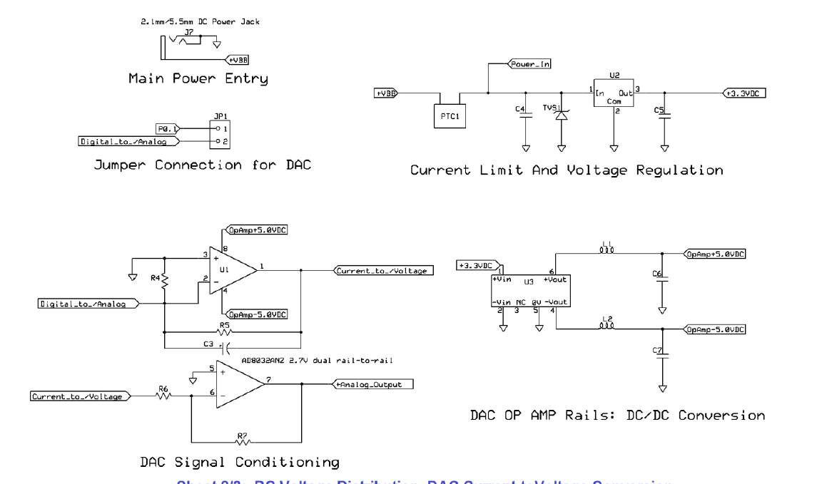
Figure 3 shows the DC voltage distribution for the C51 Microcontroller Project Launcher. The source voltage to the module (+VBB) can range from +9.0VDC to +18.0VDC, with a recommended value of +12.0VDC. The recommended +VBB connection method is to plug a regulated +12VDC Wall Adapter, such as the MEAN WELL 709-GST25U12-P1J, into DC power jack J7. (The AC adapter serving as the power source must have a 2.1mm/5.5mm center-positive output plug to be compatible with connector J7.) The advantage of using J7 as the +VBB connection point is that input current must pass through polyswitch resettable fuse PT1. If input current exceeds the 500mA hold current level of PTC1, the fuse switches into its high ohmic condition, inhibiting the flow of current to the board’s Power_In bus. (Once PTC1 enters a high-ohmic state, power must be removed from the board and the overcurrent condition must be eliminated prior to reapplication of +VBB.) Note that, in Figure 3, pad locations along the Power_In bus are highlighted in blue.
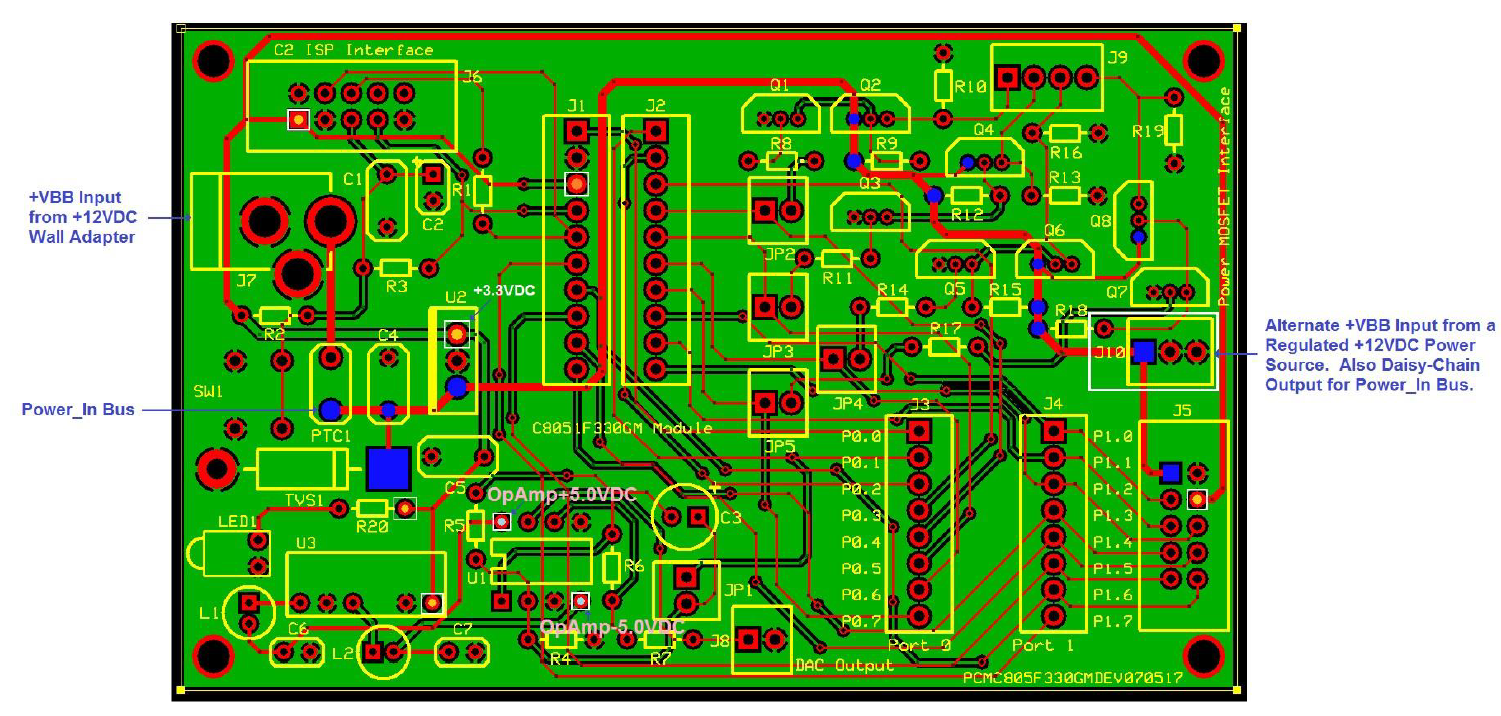
An alternate connection point for +VBB is pin strip header J10 (highlighted by a white rectangle at the RH side of Figure 3). Connecting +VBB to pin 1 of J10 (with ground at either pin 2 or pin 3) brings the source voltage directly to the Power_In bus. It should be noted that, with this power connection, PTC1 is essentially removed from the circuit and unable to serve as a current limiter. If J7 becomes the +12.0VDC input, then J10 can serve as a daisy chaining output, providing +12.0VDC to other circuit boards, assuming the total power bus current is held below 500mA (the trip point for PTC1).
As seen in Figure 3 and the schematic section in Figure 4, transient voltage suppressor TVS1 performs a voltage limiting action, clipping any transient voltage spikes on the Power_In bus that begin to exceed its 28V VRM (maximum reverse voltage). MLCC (multilayer ceramic capacitor) C4 performs an additional filtering action, reducing high frequency noise that could be present on the Power_In bus. C4 also serves as the stabilizing input capacitor for +3.3VDC regulator U2.

As indicated in Figures 3 and 4, pin 3 of voltage regulator U2 serves as the source of the +3.3VDC bus for C51 Microcontroller Project Launcher. Upon application of power, PCB indicator LED1 should illuminate, indicating the presence of +3.3VDC at the output of U2. Capacitor C5 provides noise reduction and stabilization for the +3.3VDC bus. Note that, in Figure 3, significant pad locations on the +3.3VDC bus are indicated with white rectangles and highlighted in orange. +3.3VDC at pin 1 of JTAG header J6 provides power to a debug adapter that might require a +3.3VDC power source. (The debug adapter is used during in-system programming (ISP) of the C51 Microcontroller Project Launcher Circuit Module.) Pad location 3 of J1 provides +3.3VDC to the C8051330GM DIP-20 MCU Module while it is inserted into its socket.
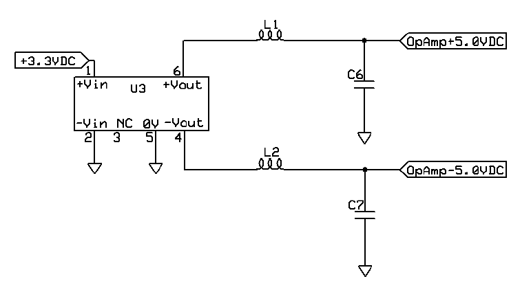
As shown in Figures 3 and 5, +3.3V is bussed to pin 1 of DC/DC power converter U3. This device, in turn, provides rail voltages +/-5.0VDC to the op amp current-to-voltage conversion circuitry of the C51 Microcontroller Project Launcher. As indicated in Figure 3, the Power_In bus voltage and +3.3VDC present at pins 1 and 4 of connector J5 allow daisy chaining of DC power to the PRESSON Microcontroller Display Circuit Module. This module interfaces with the C51 Microcontroller Project Launcher via a 10-position ribbon cable (contained in the Microcontroller Display Circuit Module Ancillary Kit).
Module Socket and I/O Port Breakout Connections #
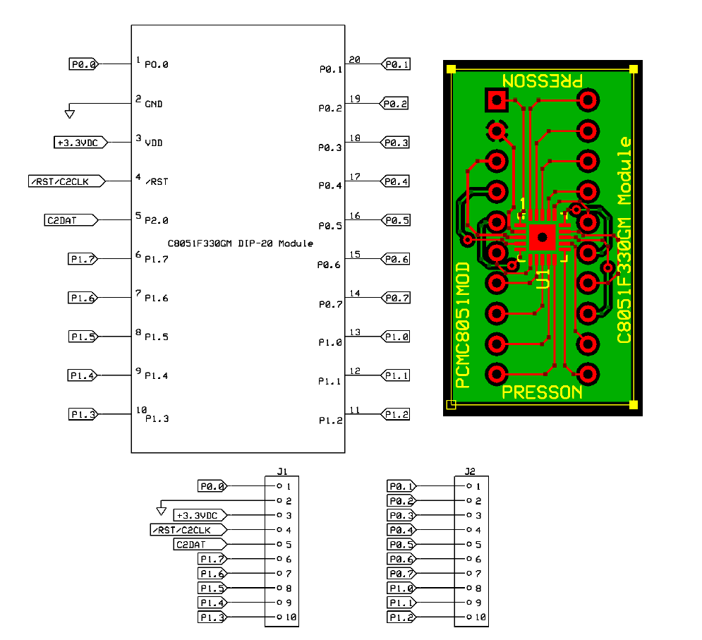
Figure 6 shows the designators for the pad locations of J1 and J2. These designations correspond to the pin locations of the C8051330GM DIP-20 MCU Module, which fits into either a standard DIP-20 IC socket or a ZIF socket during in-system programming. Note that ZIF1 (recommended for production programming) is soldered into the pad locations of J1 and J2. Figure 7 shows the silkscreen layer of the C8051330GM DIP-20 MCU Module.
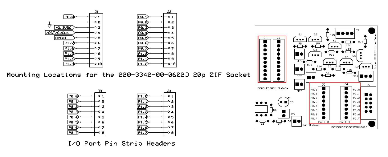
The two eight position pin strip headers, J3 and J4, serve as breakout locations for the two 8-bit MCU ports, Port 0 and Port 1. The bitwise notation used in programming the ports of the C8051F330-GM is as follows: Bit 0 of Port 0 is designated as P0.0. Bit 3 of Port 1 is designated as P1.3. (Note that, because the least significant bit position of a port is designated as 0 (representing 20), P1.3 is the fourth bit position of Port 1.) It is common to refer to port bit 0 as the LSB (least significant bit) and bit 7 of an eight-bit port as the MSB (most significant bit).
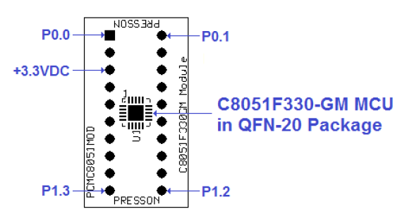
The relationship of the C8051330GM DIP-20 MCU Module, shown in Figure 7, and the J3 and J4 breakout headers might best be illustrated with an example. Assume, as shown in Figure 8, the C8051330GM DIP-20 MCU Module is inserted in the ZIF socket and running a program that produces a logic high at port bit P1.2. This high transition also occurs at pin 3 of pin strip header J4, which is the breakout point for P1.2. Also assume a jumper wire is connected between pin 3 of J4 and the base resistor of a common emitter transistor switch fabricated on the user’s breadboard. The anticipated +3.0V logic high at P1.2 turns on transistor Q1 and illuminates LED1.
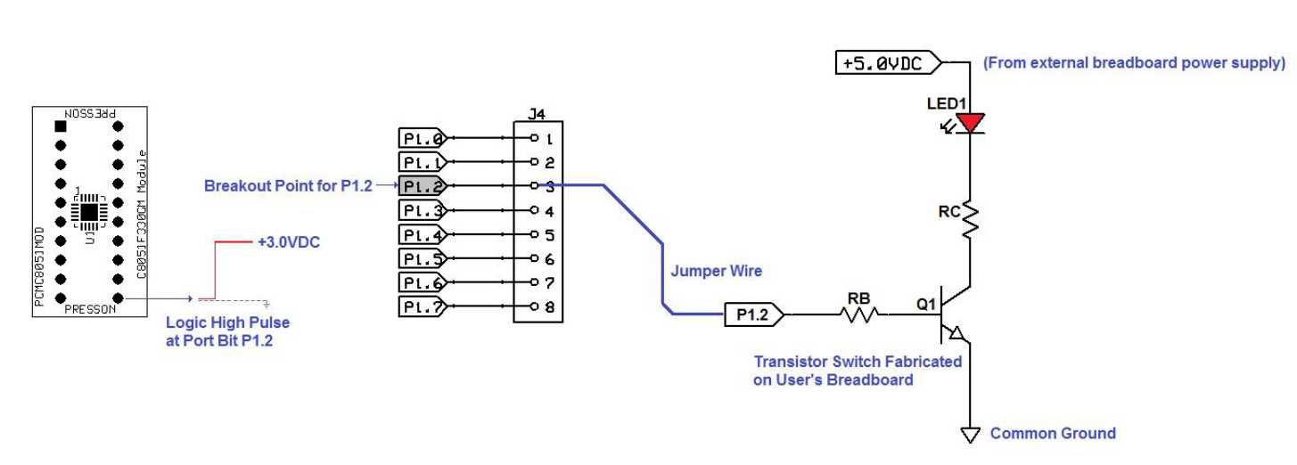
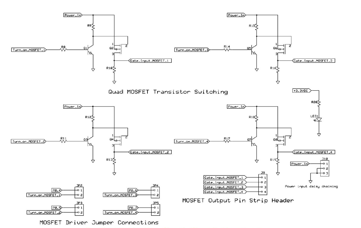
As seen in Figures 6 and 8, the presence of the J3 and J4 breakout headers on the C8051F330GM Development Board allows easy access to the sixteen individual bit locations of Ports 0 and Port 1 of the C8051F330-GM MCU. The C51 Microcontroller Project Launcher is designed specifically for training in industrial applications of an 8-bit MCU. In the field of industrial mechatronics, bitwise output programming is an essential element in controlling industrial motors and other forms of electromechanical actuator. For this reason, a Quad MOSFET Transistor Switching system has been designed directly into the C51 Microcontroller Project Launcher. Figure 9 contains a schematic diagram of this switching circuitry.
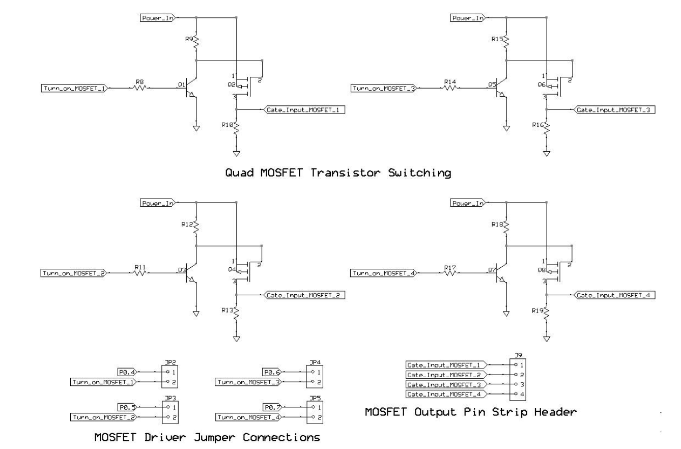
With port bits P0.4, P0.5, P0.6, and P0.7 present at pins 5, 6, 7, and 8 of header J3, these four port bits can also become the inputs to the four transistor switching channels. This transistor switching circuitry is designed to provide a safe interface between the C8051330GM DIP-20 MCU Module and external n-channel power MOSFET transistors that could be used to commutate higher power loads such as motors and solenoids. Jumper positions JP2, JP3, JP4, and JP5 allow access to these four transistor output channels. Each jumper position contains a two-position pin header. Placing a shorting jumper over one of these headers allows its associated port bit to become the control input to a two-stage level shifting transistor switch.
For example, placing a shorting jumper over JP2 allows an output the P0.4 bit position to function as the Turn_on_MOSFET_1 signal. A logic high at P0.4 turns on transistor Q1. With Q1 in a saturation state, the voltage at the gate of p-channel MOSFET Q2 is nearly +0.2VDC. This low gate voltage switches Q2 into full conduction, bringing the Gate_Input_MOSFET_1 signal (at pin 1 of header J9) to nearly the level of Power_In. This signal could be sent to the gate of an external n-channel power MOSFET which could function as a current sinking switch for a high-power electromechanical load. The action just described would be identical for the remaining three output channels, as shown in Figures 9 and 10. Also, as shown in Figures 9 and 10, four position pin header J9 serves as the interface point for connection to four external power MOSFETs.
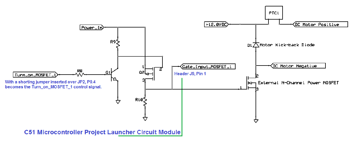
The relationship of the C8051330GM DIP-20 MCU Module, transistor switching channels, and external power circuitry might best be illustrated with an example. Assume a shorting jumper has been placed over the JP2 header, as described in Figure 11. This allows P0.4 to become the controlling input for the Gate_Input_MOSFET_1 output channel. If the program currently running on the C8051330GM DIP-20 MCU Module brings P0.4 to a logic high, then the nearly +3.0V level of the Turn_on_MOSFET_1 signal brings the Gate_Input_MOSFET_1 output to nearly the level of Power_In. Assuming Power_In is +12.0VDC, then this voltage level at pin 1 of J9 is sufficient to drive the external MOSFET into full conduction. With the external MOSFET functioning as a closed switch, nearly +12.0V develops between the positive and negative terminals of the DC motor. It should be noted that a power MOSFET, such as the Nexperia PSMN4R330PL, can sink nearly 100 amperes of current when in full conduction. Also, this MOSFET is capable of very fast commutation. The C8051330GM DIP-20 MCU Module could be programmed to provide a pulse width modulated signal at its P0.4 output, allowing the MCU to precisely control motor speed.
DAC Signal Conditioning #
The C8051F330-GM MCU contains a current mode digital-to-analog converter (IDAC), which is accessible at the P0.1 output (pin 20 of the C8051330GM DIP-20 MCU Module). When configured to operate as the IDAC output, P0.1 converts changes in a 10-bit binary control number (placed in the IDAC high and low input registers during programming) to proportional changes in output current at P0.1. With a 10-bit binary input, the IDAC can produce up to 1024 gradations of output current.
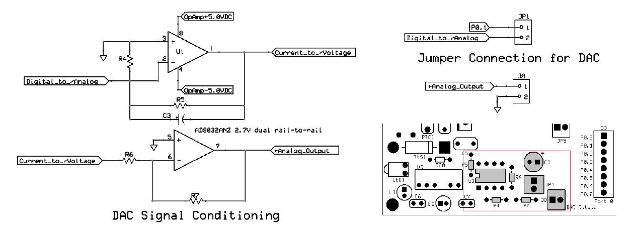
As shown in Figure 12, the C51 Microcontroller Project Launcher Circuit Module contains dual op amp signal conditioning circuitry that converts changes in current at P0.1 to changes in the analog voltage at pin 7 of U1. Assuming P0.1 has already been configured by firmware to function as the IDAC output, the current-to-voltage conversion circuitry is accessed by inserting a shorting jumper over header JP1. This allows the IDAC output, designated as Digital_to_/Analog, to function as the current source for the integrator formed by the first op amp stage. An increase in IDAC current causes an increase in negative potential at the Current_to_/Voltage point. The second op amp stage functions as a simple inverting amplifier, allowing the +Analog_Output signal to develop between 0V and nearly +5.0VDC as the IDAC output current varies between 0 amps and a maximum value specified through MCU programming. As shown in Figure 12, the +Analog_Output signal is taken at output header J8 on the C51 Microcontroller Project Launcher.
Microcontroller Display Module Interface #
The C51 Microcontroller Project Launcher provides a convenient ribbon cable connection to the PRESSON Microcontroller Display Module. Purchase of the display module, shown in Figure 14, is highly recommended for students completing the PRESSON courseware involving analog-to-digital conversion and sensor signal conditioning. A three-digit seven-segment display multiplexing routine is included with the downloadable source code for the C51 Microcontroller Project Launcher. This code has been written specifically for operation of the three-digit seven segment display contained on the Microcontroller Display Module. Thus, the pin assignments for dual-row JTAG header J5 shown in Figure 13 conform to the port bit assignments given in the display multiplexing routine. Connection of a ten-position ribbon cable from J5 of the C51 Microcontroller Project Launcher Circuit Module to J1 of the Microcontroller Display Module provides power to the display circuitry and allows implementation of the three-digit seven segment display multiplexing routine using the C8051330GM DIP-20 MCU Module. (This ribbon cable is provided with the Microcontroller Display Module Ancillary Kit.)

Note, as shown in Figure 14, the three-digit seven segment display is attached to the ground plane side of the PCB. The Microcontroller Display Board also contains an eight-position bitwise LED display, located on the silkscreen side of the PCB. The transistor drivers for these LEDs are accessed independently. As an example, to indicate the logic state of a port bit of the C8051330GM DIP-20 MCU Module, the user could make a quick jumper connection from a pin of header J3 or J4 on the C51 Microcontroller Project Launcher to one of the bitwise connection points on header J3 of the Microcontroller Display Module. (A common ground connection must also exist between the two circuit modules.)

C2 In-System Programming Interface and Reset Circuitry #
Figure 15 shows the locations and pin-out of the in-system programming (ISP) interface and Manual Reset circuitry for the C8051F330GM Development Board. Dual row/10-position header J6 is used to attach the Silicon Labs 8-Bit USB Debug Adapter (Mouser part number 634-DEBUGADPTR1USB) to the C51 Microcontroller Project Launcher Circuit Module. Tactile switch SW1 serves as the Manual Reset for the project launcher.

The ISP interface on the C51 Microcontroller Project Launcher Circuit Module is compatible with both the Silicon Labs 8-Bit USB Debug Adapter and the older Serial Debug Adapter. The USB Debug Adapter provides +5.0VDC at pin 10 of its JTAG output connector allowing it to become the power source for its target board. However, because the C8051330GM DIP-20 MCU Circuit Module has its own internal power bussing, the pin 10 connection of J6 on the C8051F330GM Development Board is left open. The older serial version of the Silicon Labs Debug Adapter relies on its target for DC operating voltage. For this reason, the C8051F330GM Development Board provides a +3.3VDC power source for that adapter at pin 1 of J6. Because pin 1 of the USB adapter’s output connector is open, the +3.3VDC from the development board is isolated from that device. While the ISP interface is not in use, pin 1 of J6 could serve as a temporary +3.3VDC power source for external circuitry, with a common ground connection available at either pin 2 or pin 3 of header J10.
Performing programming exercises for the C51 Microcontroller Project Launcher Circuit Module with the Silicon Labs IDE requires use of the Silicon Labs USB Debug Adapter, which connects between the USB port of the user’s PC and J6 of the C51 Microcontroller Project Launcher Circuit Module. The USB Debug Adapter, available through Mouser electronics, must be purchased separately. The Silicon Labs IDE and the most recent PDF courseware and documentation for all PRESSON products are stored on a flash drive. This flash drive is included with a customer’s first PRESSON product purchase.
Appendix 1 #
System Schematic Diagrams C8051330GM DIP-20 MCU Circuit Module Pin Out:
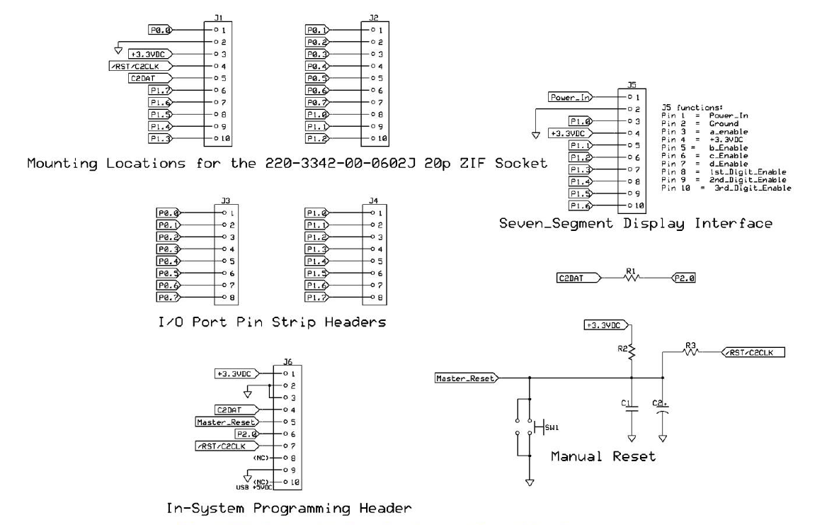
C51 Microcontroller Project Launcher Circuit Module Schematic Diagrams
Appendix 2 #
| Table 2 – Bill of Materials | ||
|---|---|---|
| Component | Description | Product Number |
| C1 | 0.47uF 50V 20% ZFU MLCC | 80-C322C474M5U |
| C2 | 1uF 35V 20% tantalum | 581-TAP105M035SCS |
| C3 | 47uF 10V 20% organic polymer | 661-PSA10VB47M |
| C4 | 0.33uF 50V 20% Z5U MLCC | 80-C322C334M5U |
| C5 | 0.47uF 50V 20% ZFU MLCC | 80-C322C474M5U |
| C6 | 2.2uF 16V 10% X7R MLCC | 810-FK14X7R1C225K |
| C7 | 2.2uF 16V 10% X7R MLCC | 810-FK14X7R1C225K |
| J3 | 8p 0.1″ pin strip header | 571-6404528 |
| J4 | 8p 0.1″ pin strip header | 571-6404528 |
| J5 | 10p JTAG header | 571-5-146256-5 |
| J6 | 10p JTAG header | 571-5-146256-5 |
| J7 | 2.0mm/5.5mm DC Jack | 806-KLDX-0202-A-LT |
| J8 | 2p 0.1″ pin strip header | 571-6404522 |
| J9 | 4p 0.1″ pin strip header | 571-6404524 |
| J10 | 3p 0.1″ pin strip header | 571-6404523 |
| JP1 | 2p 0.1″ pin strip header | 571-6404522 |
| JP2 | 2p 0.1″ pin strip header | 571-6404522 |
| JP3 | 2p 0.1″ pin strip header | 571-6404522 |
| JP4 | 2p 0.1″ pin strip header | 571-6404522 |
| JP5 | 2p 0.1″ pin strip header | 571-6404522 |
| L1 | 22uH 0.95ohm 10% | 580-11R223C |
| L2 | 22uH 0.95ohm 10% | 580-11R223C |
| LED1 | 3mm (T-1) red (700nm) 6 mcd CBI | 749-H101CRD |
| PTC1 | PTC Fuse 0.5A hold current 1 A trip current | 650-RXEF050 |
| Q1 | MPSA20 npn small signal | G19467 |
| Q2 | 40V P-channel enhancement RDS(on) = 8ohm | 689-VP0104N3-G |
| Q3 | MPSA20 npn small signal | G19467 |
| Q4 | 40V P-channel enhancement RDS(on) = 8ohm | 689-VP0104N3-G |
| Q5 | MPSA20 npn small signal | G19467 |
| Q6 | 40V P-channel enhancement RDS(on) = 8ohm | 689-VP0104N3-G |
| Q7 | MPSA20 npn small signal | G19467 |
| Q8 | 40V P-channel enhancement RDS(on) = 8ohm | 689-VP0104N3-G |
| R1 | 1Kohm 1/8W metal film | 270-1K-RC |
| R2 | 2.2Kohm 1/8W 1% metal film | 270-2.2K-RC |
| R3 | 6.8Kohm 1/8W 1% metal film | 270-6.8K-RC |
| R4 | 1.5Mohm 1/8W 1% metal film | 270-1.5M-RC |
| R5 | 3.3Kohm 1/8W 1% metal film | 270-3.3K-RC |
| R6 | 1.5Kohm, 1/8W 1% metal film | 270-1.5K-RC |
| R7 | 4.7Kohm 1/8W 1% metal film | 270-4.7K-RC |
| R8 | 12Kohm 1/8W 1% metal film | 270-12K-RC |
| R9 | 1Kohm 1/8W 1% metal film | 270-1K-RC |
| R10 | 1Kohm 1/8W 1% metal film | 270-1K-RC |
| R11 | 12Kohm 1/8W 1% metal film | 270-12K-RC |
| R12 | 1Kohm 1/8W 1% metal film | 270-1K-RC |
| R13 | 1Kohm 1/8W 1% metal film | 270-1K-RC |
| R14 | 12Kohm 1/8W 1% metal film | 270-12K-RC |
| R15 | 1Kohm 1/8W 1% metal film | 270-1K-RC |
| R16 | 1Kohm 1/8W 1% metal film | 270-1K-RC |
| R17 | 12Kohm 1/8W 1% metal film | 270-12K-RC |
| R18 | 1Kohm 1/8W 1% metal film | 270-1K-RC |
| R19 | 1Kohm 1/8W 1% metal film | 270-1K-RC |
| R20 | 82ohm 1/8W 1% metal film | 270-82-RC |
| ZIF1 | 20p ZIF socket for C8051F330GM Module | 517-220-3342-00 |
| DIP1 | 8p DIP socket | 571-2-1571552-2 |
| SW1 | NO momentary tactile | 653-B3W-1002 |
| TVS1 | 15V unidirectional transient suppressor | 511-BZW06-28 |
| U1 | AD8032ANZ 2.7V dual rail-to-rail op amp | 584-AD8032ANZ |
| U2 | 3.3VDC 500mA regulator | 595-UA78M33CKCSE3 |
| U3 | 3.3VDC in to +/-5.0VDC out DC/DC converter | 580-NKA0305SC |
| C8051DevPCB | 4.0″ x 2.5″ two-layer FR-4 epoxy glass PCB | PCMC805F330DEV070517 |
NOTE: One C8051330GM DIP-20 MCU Module is included with the PRESSON C51 Microcontroller Project Launcher. Extra pieces of the C8051330GM DIP-20 MCU Module can be purchased directly from PRESSON Circuit Modules, Inc.
Appendix 3 #
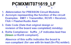
Anatomy of a PRESSON PCB Stock Number
